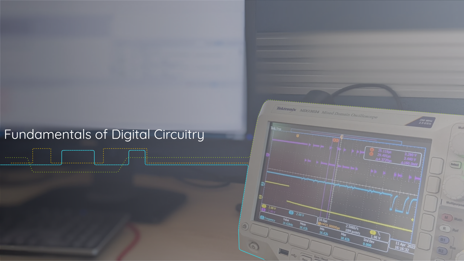
Fundamentals of Digital Circuitry
Introduction
In this piece, we will explore the fundamental concepts of digital electronics, including logic levels, push-pull and open-drain configurations, pull-up and pull-down resistors, and the Schmitt trigger. Our objective is to provide a comprehensive and in-depth understanding of these essential concepts and their practical applications in GPIOs of microcontrollers and digital communication protocols such as I2C and SPI. Through clear explanations and practical examples, we aim to equip readers with the knowledge and expertise needed to understand the workings of digital ports and buses and effectively utilize their capabilities in different electronic systems.
Logic Levels
In digital electronics, information is represented and processed using binary voltage levels: everything hence boils down to the voltage being or not being present. To accomplish that, two voltage levels are used to distinguish between the two binary states, typically represented as 0 and 1, or Logical Low and Logical High.
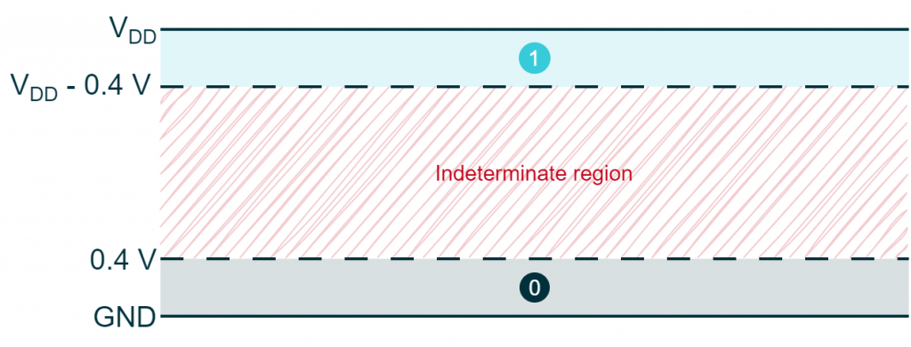
The specific voltage ranges that represent each of these states are defined by the threshold or trip points of the logic. To ensure the accuracy of digital signals, the trip points are chosen to be far apart from each other and to minimize the chance of errors due to noise or signal distortions. For example, in a CMOS microcontroller, the logic levels are defined such that a voltage of 0V represents a logical 0 and a VDD represents a logical 1. However, to account for variations in voltage levels, a margin of acceptable voltage levels is also defined.
If in this example the supply voltage (VDD) is 3.3V, any voltage between 2.9V and 3.3V would be considered a logical 1 and any voltage between 0V and 0.4V would be considered a logical 0. In case the voltage should land in the indeterminate region, the behavior of the logic would be unpredictable, hence, signals in this area are not acceptable.
Switch level models
The implementation of digital circuits relies mostly on transistors being used as switches. In this scenario, a transistor can be seen as a switch driven by a digital signal often in conjunction with capacitors or resistors to model loads, losses and transients. From this perspective, a transistor can be modeled as an active high or active low switch. These special switches will then have three terminals, one of which is used to electrically control it.
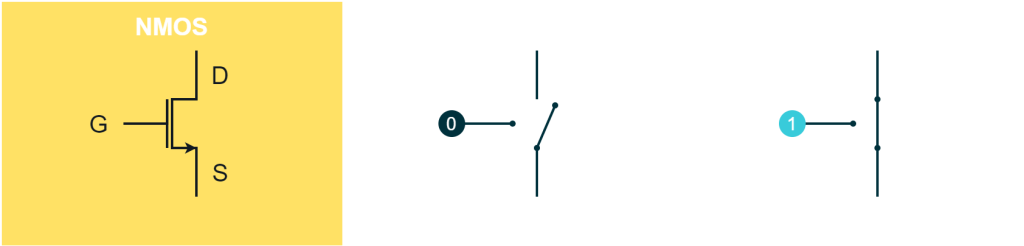
An active high switch operates by closing when a logical 1 is applied to its control terminal and opening when a logical 0 is applied. This type of switch is typically implemented using an NMOS transistor.
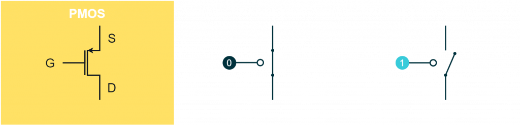
Similarly, an active low switch operates by closing when a logical 0 is applied to its control terminal and opening when a logical 1 is applied. This type of switch is typically implemented using a PMOS transistor. Note that the circle on the control terminal highlights the inverted logic of this type of switch and will be used throughout this article to highlight the nature of the switch.
Push-pull configuration
The simplest and most used configuration that can be implemented by combining two switches of different natures is the push-pull configuration. In this configuration one switch is “pushing” current in one direction and the other switch is “pulling” current in the opposite direction. This arrangement allows a bi-directional current flow while providing isolation between the control and output signals.
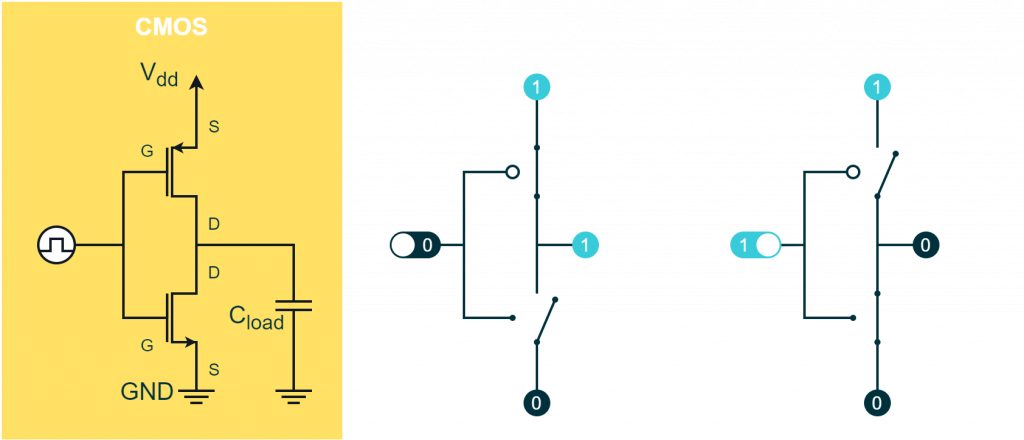
In this configuration, the control inputs of the two switches are connected together and driven by the same signal. Depending on the logic level applied to the control input, we have two possible outcomes:
- If the input is low then the high side switch is closed and the low side is open. Consequently, a current is pushed in the load until the output reaches the high logical state
- If the input is high then the low side switch is closed and the high side is open. In this case, a current is pulled out from the load until the output reaches the low logical state
The push-pull configuration is often used as a NOT gate, as it outputs the negation of the input. This configuration offers isolation between the control signal and the output signal, as the current that flows into the load is sourced from the supply. This mechanism relies on the transistor effect where a small current flow allows to control of a large current flow. For example, the input signal may only draw micro or nano-amperes of current, while the output can drive a milli-ampere-consuming LED without affecting the control signal.
Open-drain configuration
The open-drain configuration is used in scenarios where multiple devices are connected on a shared line for communication purposes. In this case, using a push-pull configuration to drive the line to a logic 1 or 0 is not feasible, as it can result in a short circuit if two devices try to drive the line high and low simultaneously.
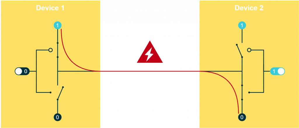
The open-drain configuration solves this issue by eliminating the high side switch and leaving the drain of the NMOS open (from here the name open-drain or sometimes open-collector with reference to the BJT transistor). This allows each device to pull the signal low by connecting it to the ground, while, when none of the devices are pulling low, the signal line is left floating and can be pulled high by a pull-up resistor.
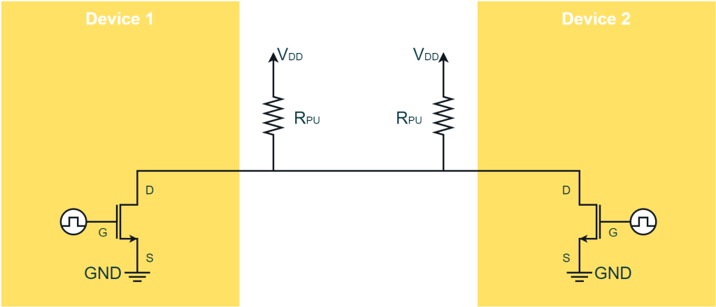
The open-drain configuration is commonly used in half-duplex digital communication buses such as I2C, as it allows multiple devices to communicate on the same bus without interfering with each other.
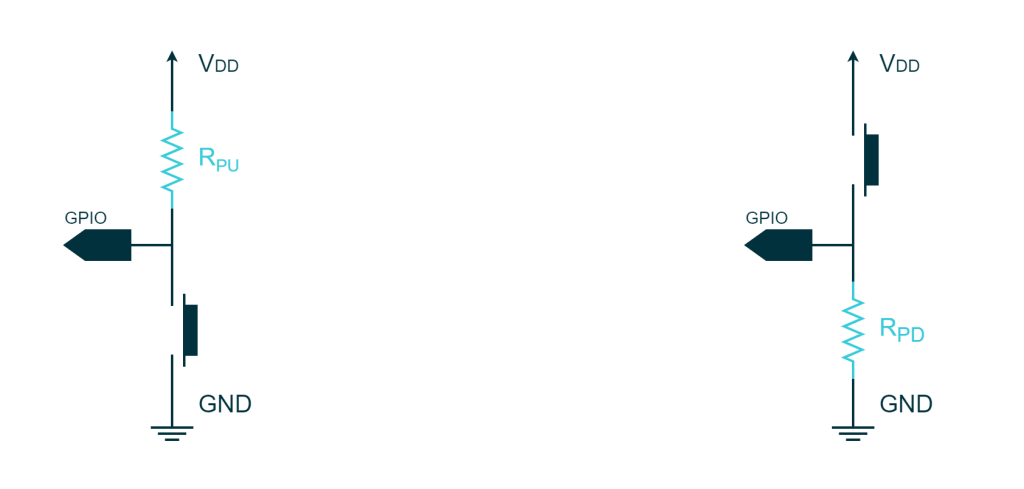
Pull-up and Pull-down resistors
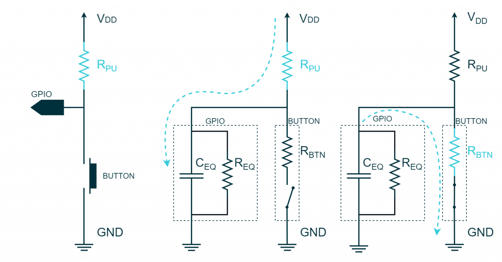
In digital circuits, resistors are sometimes used to maintain a defined logic level on a signal line. If an active pull is not suitable (e.g in the previously shown open-drain configuration) these resistors can be utilized. They are called pull-up resistors when connected to the VDD side of the line and pull-down resistors when connected to the GND side. For example, a pull-up resistor on the input port can ensure that the line stays high even when nothing is connected to the bus.
A common application of pull-up and pull-down resistors is in conjunction with buttons. In the following illustration, a push button is connected to an input pin in two possible configurations. The left diagram shows the button connected on the low side: when it is pressed, the line is pulled low and when released, the line is pulled up by the pull-up resistor. In contrast, the right diagram depicts the button on the high side and the resistor on the low side: in this case, the resistor is responsible for pulling down the line when the button is not pressed.
Determining the pull resistor size
The choice of the size of a pull resistor is influenced by several constraints. Firstly, it must be strong enough to pull the signal to the desired voltage level when the line is not actively driven by a device. On the other hand, it must be weak enough to allow a device to drive the signal to the opposite level when needed. Additionally, the size of the pull resistor affects the rise and fall time of the signal: this is an important consideration to make when designing the system in order to ensure that it meets the timing requirements. Finally, the power consumption must be taken into account so the value should be chosen such that it does not exceed the power dissipation limit of the resistor or the device.
To analyze the problem let us consider the button example with a pull-up resistor. In this scenario, the GPIO can be modeled as an equivalent capacitor CEQ in parallel to a load resistor REQ: more specifically this capacitor will take into account both the input capacitance of the GPIO (CINT) and the parasitic capacitance of the line (CEXT); the equivalent resistor instead models the internal losses. The voltage on the capacitor represents the voltage read by the GPIO: the game is to load the capacitor to VDD to get a logical 1 or discharge it to Ground to get a logical 0. The button can be modeled as an ideal switch in series with a resistor RBTN that represents the resistance offered by the button when closed.
Strength and weakness
In a real-world scenario, the resistance value of REQ is usually so high that it can be considered open, and the resistance value of RBTN is so low that it can be considered a short circuit. However, for the purpose of this analysis, let us examine their contribution when the button is pressed or released.
When the button is not pressed, the capacitor is charged through the pull-up resistor RPU to 
On the other hand, when the button is pressed, the capacitor discharges to 
Let us now consider the non-ideal case where RBTN is 150Ω and REQ is 1MΩ and see how VLOW and VHIGH change depending on the value of RPU if VDD were 3.3V.
| RPU [Ω] | VLOW [V] | VHIGH [V] |
|---|---|---|
| 500 | 0.76 | 3.30 |
| 600 | 0.66 | 3.30 |
| 700 | 0.58 | 3.30 |
| 800 | 0.52 | 3.30 |
| 900 | 0.47 | 3.30 |
| 1k | 0.43 | 3.30 |
| 2k | 0.23 | 3.29 |
| 5k | 0.10 | 3.28 |
| 10k | 0.05 | 3.27 |
| 100k | 0.00 | 3.00 |
| 150k | 0.00 | 2.87 |
| 200k | 0.00 | 2.75 |
| 300k | 0.00 | 2.54 |
| 400k | 0.00 | 2.36 |
This table illustrates the concept of classifying a pull resistor as weak or strong.
A low-value resistor exerts a strong pull towards its side. In this scenario, where our poor button is pressed, a 1KΩ pull-up resistor is strong enough to move the VLOW into the indeterminate region (we defined it in the first chapter as being between 0.4 and 2.9V). On the other hand, when the button is not pressed, a strong pull-up resistor maintains the VHIGH quite healthy even if our GPIO exhibits a large current loss of 3.3uA (
Conversely, a high-value resistor pulls weakly towards its side. It struggles to keep the VHIGH when the button is open due to the high current loss (i.e. REQ is too small). For instance, a 150KΩ pull-up resistor is already too weak in this scenario. On the other hand, a weak pull-up resistor makes it easier for the button to pull down the line when it is pressed.
This use case was quite exaggerated for the purpose of the analysis. In reality, we can easily expect a button resistance (RBTN) as small as 10Ω and a GPIO parasitic resistance (REQ) as large as 10MΩ. In such a case, our calculation would yield as follow.
| RPU [Ω] | VLOW [V] | VHIGH [V] |
|---|---|---|
| 500 | 0.065 | 3.300 |
| 600 | 0.054 | 3.300 |
| 700 | 0.046 | 3.300 |
| 800 | 0.041 | 3.300 |
| 900 | 0.036 | 3.300 |
| 1k | 0.033 | 3.30 |
| 2k | 0.016 | 3.299 |
| 5k | 0.007 | 3.298 |
| 10k | 0.003 | 3.297 |
| 100k | 0.000 | 3.267 |
| 150k | 0.000 | 3.251 |
| 200k | 0.000 | 3.235 |
| 300k | 0.000 | 3.204 |
| 400k | 0.000 | 3.173 |
This table shows that, even with the weakest (400 kΩ) and strongest (500 Ω) pull-up resistors that we have considered, the thresholds are good enough in terms of voltage levels.
Transient speed and current
For the subsequent portion of the analysis, we will examine the impact of the pull-up resistor on the rising time and power consumption. Note that the same analysis would apply to the falling time in the case of a pull-down resistor. This analysis will be based on a fully discharged capacitor (worst-case scenario) and disregards the effect of REQ. Our focus will be solely on the rising time, which is the parameter influenced by the choice of the pull-up resistor. The relevant equations, which are derived in the appendix, are:


In the context of our case study, these equations become:


Before proceeding with the analysis some details about CEQ need to be discussed. As mentioned before, this capacitance takes into account both the input capacitance of the GPIO (CINT) and the parasitic capacitance of the line (CEXT). Hence, its total value would be

The first, CINT, depends on the technology and the manufacturer of the MCU whose GPIO is being considered. To provide some references, examples of input capacitance values for popular microcontrollers are:
- Atmel ATmega328P (Arduino Uno): 6-8 pF
- STMicroelectronics STM32F030F4P6: 6-9 pF
- NXP Semiconductors LPC11U24F: 4-7 pF
The second, CEXT, depends on several factors such as the trace width, dielectric constant, and the material used as a substrate when the MCU is soldered on a PCB. For a standard FR-4 substrate with a dielectric constant of 4.5 and a trace width of 10mil (0.25mm), the line capacitance can be estimated to be around 3-5pF per cm. So, for a 5cm trace, the capacitance would be around 15-25pF.
In summary, if we consider a CEQ of 50pF, we have been very conservative about the quality of both our MCU and PCB.
The following table reports the time it takes for the GPIO to reach 95% (i.e. 3 time-constants) and 99% (i.e. 5 time-constants) of the steady-state voltage with a VDD of 3.3V and CEQ of 50pF. It also includes the maximum current and power drawn over the pull-up resistor RPU, as the value of the resistor varies.
| RPU [Ω] | 95% transient (3 RC) [uS] | 99% transient (5 RC) [uS] | IMAX [mA] | PMAX [mW] |
|---|---|---|---|---|
| 500 | 0.075 | 0.125 | 6.6 | 21.78 |
| 600 | 0.09 | 0.15 | 5.5 | 18.15 |
| 700 | 0.105 | 0.175 | 4.71 | 15.56 |
| 800 | 0.12 | 0.2 | 4.12 | 13.61 |
| 900 | 0.135 | 0.225 | 3.67 | 12.10 |
| 1k | 0.15 | 0.25 | 3.30 | 10.89 |
| 2k | 0.3 | 0.5 | 1.65 | 5.45 |
| 5k | 0.75 | 1.25 | 0.66 | 2.18 |
| 10k | 1.5 | 2.5 | 0.33 | 1.09 |
| 100k | 15.00 | 25 | 0.033 | 0.11 |
| 150k | 22.5 | 37.5 | 0.022 | 0.07 |
| 200k | 30 | 50 | 0.017 | 0.05 |
| 300k | 45 | 75 | 0.011 | 0.04 |
| 400k | 60 | 100 | 0.008 | 0.03 |
At the extreme of this analysis, there is a very strong 500Ω pull-up resistor that consumes nearly 1/4 watt and allows the line to reach 95% of its final value within 125 nanoseconds. Opting for this resistor means prioritizing speed over using larger components capable of handling the resulting high current.
On the other hand, a pull-up resistor of 400kΩ is extremely weak and takes 60us for the line to reach 95% of its final value, with a negligible current. A rising time of 60us may not be an issue if the application involves a button, however, if we are considering an I2C bus running at a minimum of 100kHz, the 10us period of the clock line combined with a CEQ of 50pF makes it unsuitable.
So what is the best choice? It ultimately depends on the specific application, but in general, pull resistors in the range of 1kΩ to 10kΩ are acceptable for a wide range of applications.
The benefits of using a Schmitt Trigger
In the world of digital electronics, signals often suffer from noise and interference, causing them to be unreliable. To tackle this issue, engineers often turn to a circuit called a Schmitt Trigger. The Schmitt Trigger acts as a filter, cleaning up a noisy digital signal and providing a reliable output. In this paragraph, we will delve into the details of how a Schmitt Trigger works and the benefits it offers in improving the quality of digital signals.
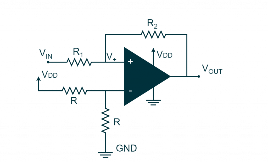
This circuit is implemented using an operational amplifier and a positive feedback loop. The output of this circuit can be only in two states: if the input is greater than the upper threshold (VTH) the output will be VDD. Conversely, if the input is less than the lower threshold (VTL) the output will be Ground. The following formulas can be used to calculate the thresholds.


If we set R2 to 3kΩ and R1 to 1kΩ the thresholds will then be


The following picture shows the output of the Schmitt trigger when the input is a sinusoid with an offset of VDD/2 and a peak-to-peak value of VDD.
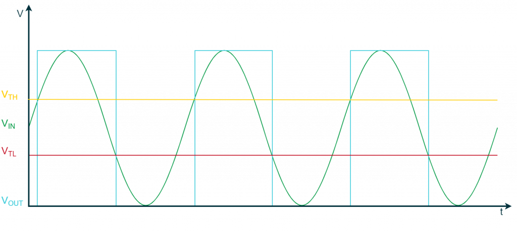
This brings us to a real case scenario where an input port of a microcontroller receives a quite noisy signal. The following figure shows how the Schmitt Trigger tackles this issue (move the slider to do a comparison with and without the trigger).


Concluding, is quite typical nowadays that many microcontrollers filter digital inputs using a Schmitt Trigger to clean up a noisy digital signal and provide reliable behavior of their GPIO.
Appendix A
In this appendix, we are going to solve the equation of an RC circuit and draw some conclusions.
First-order non-homogenous differential equation with constant coefficients
Let us consider the equation

that is a first-order non-homogenous differential equation with constant coefficients.
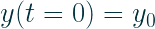
The solution to this equation is a family of functions. To find a unique solution, a boundary condition is needed such as the value of y at a specific time. For convenience, the time chosen is 0 as we will see it simplifies the math.
The homogeneous solution can be found by rearranging the homogenous equation (b = 0), integrating both sides, and using some properties of logarithms and exponentials.


The complete solution of the original equation however is the sum of the homogeneous solution plus a particular solution. For the method of the similarities, as b is a polynomial of order zero (i.e. a constant) the particular solution is expected to be a polynomial of the same order (let us call it k2)

The first constant can be found substituting the solution in the original equation we have


The second constant can be found using the boundary condition. So imposing t = 0 yields to


hence the solution we were looking for is

First-order RC circuit
Let us consider an RC network and a voltage generator as shown in the figure.
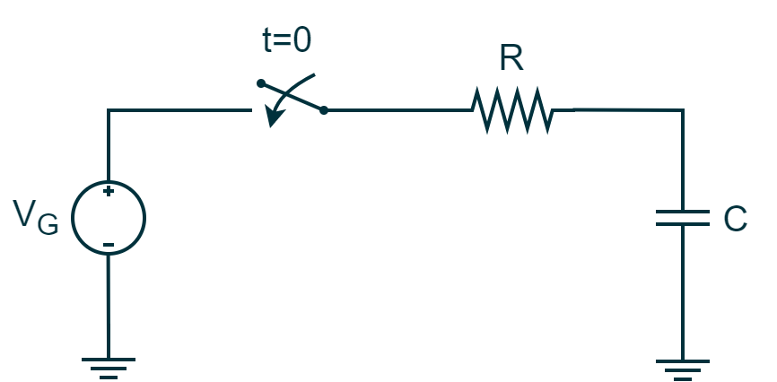
the following statements are all true:
- The DC voltage generator has an amplitude of VG
- The switch gets closed at the time t = 0
- The capacitor is preloaded to a specific voltage level VC0 before the switch gets closed
- As in the absence of infinite current, the voltage across a capacitor cannot change instantaneously we can state that in the moment the switch gets closed Vc(t = 0) is still VC0
Deriving the equation
To solve this circuit we start with the law of a capacitor

For the Kirchoff Voltage Law when the switch is closed we have


This equation is in the form
As seen in the previous paragraph, the solution to this equation is given by
that particularized to our specific case brings to
The equation can be further generalized if we consider that

Transient time
Let us plot the equation on a time chart for a fixed value of RC.
We can easily notice that the voltage goes from the initial value to the final value asymptotically. The slope of the exponential and hence the duration of the transient depends directly on the RC value. Indeed the transient is over when t >> RC and the exponential term tends to 0. For this reason, RC is often referred to as tau or time-constant. The following table shows the elapsed percentage of the transient assuming t to be multiples of RC.
| t | Exponential | Exponential value | Transient percentage |
|---|---|---|---|
| 1RC | e-1 | 0.367879 | 63.21 % |
| 2RC | e-2 | 0.135335 | 86.47 % |
| 3RC | e-3 | 0.049787 | 95.02 % |
| 4RC | e-4 | 0.018316 | 98.17 % |
| 5RC | e-5 | 0.006738 | 99.33 % |
| 6RC | e-6 | 0.002479 | 99.75 % |
| 7RC | e-7 | 0.000912 | 99.91 % |
| 8RC | e-8 | 0.000335 | 99.97 % |
Looking at the table with good approximation the transient may be considered concluded after 5 time-constants. It goes without saying that having a smaller time constant (e.g. with a fixed capacitance, a smaller resistance value) shortens the transient time.
Current
The current that flows in the circuit depends on time and can be calculated in various ways. One is to derive the current of the capacitor and this results in the following equation
The current hits its maximum value at the beginning of the transient when the capacitor is completely discharged.

In general, during a transient period of an RC circuit, a current flows through the circuit. At the start of the transient, the current is at its highest, as the voltage across the capacitor is further from the eventual steady-state voltage. The direction of the current flow is dependent on the type of transient: if the capacitor is being charged, the current flows toward the capacitor, and if the capacitor is being discharged, the current flows away from the capacitor.
The duration of the transient depends on the resistor: this component indeed limits the amount of charge that flows in and out from the capacitor (current) and ultimately the speed of the charge and discharge.
Power and Energy
In the previous chapter we have seen that when charging the capacitor, a current flows through the resistor into the capacitor. It should come as no surprise that some power is dissipated over the resistor in the process. To calculate this power let us consider once again the equation of the capacitor voltage and as we know that steady-state voltage is VG let us rewrite it

Reapplying Kirkoff voltages law we have

The power dissipated on the resistor can be calculated as 
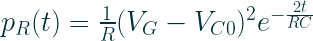
And predictably the maximum power consumption is at the beginning of the transition (t = 0) when the capacitor is totally discharged (VC0 = 0)

So, while a small resistor provides faster transients, it also requires the resistor to withstand higher power consumption. The energy on the other hand can be seen as the integral of the power in the transient
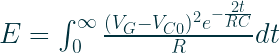

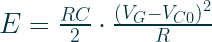

That finally shows that the amount of energy stored in the capacitor depends on its size only, while the resistance influences only the speed with which the capacitor is loaded and the overall power dissipation.
Conclusions
We can conclude this discussion with the following points. In an RC circuit:
- Smaller resistance results in a faster transient and larger resistance results in a slower transient.
- Faster transient leads to higher circuit current and thus higher maximum power dissipation.
- However, the energy of the transient is solely dependent on the capacitor and not the resistance.
Appendix B
Non-inverting single-supply Schmitt Trigger
Let us consider the following circuit composed of a single-rail operational amplifier. The non-inverting input is offset to half the rail voltage (
The working principle of this circuit is that when V+ is greater than V–, the output VOUT will reach its maximum value of VDD. Conversely, when V+ is less than V– the output will converge to Ground. This is due to the positive feedback loop that maintains saturation. The voltage level at which the output of the trigger switches, is dependent on the slope of VIN. This results in a hysteretic behavior that has many practical applications.
To determine the transfer characteristic of this circuit, we can apply the principle of superposition to the linear circuit consisting of R1 and R2. This calculation involves finding the contribution to V+ from both VIN and VOUT individually and then summing it. The math is quite trivial if we consider that no current flows in the non-inverting terminal and that a voltage generator behaves as a short circuit when turned off. The resulting equation is hence the sum of two voltage dividers:

The value of VIN that will trigger output change from low to high will be called the upper threshold (VTH). To calculate this value we need to impose some conditions on the previous equation. In this case, VOUT would be replaced with 0V, V+ to VDD/2 and VIN will represent our VTH. This yields:

Similarly to obtain VTL VOUT would be replaced with VDD. This yields:


The following picture shows the transfer function of this circuit. The yellow arrows represent the positive slope of the input signal: in this case, the input needs to reach VTH before the output switches from 0 to VDD. Conversely, when the input has a negative slope (azure arrows) the input needs to reach VTL before the output switches from VDD to 0.
Be the first to reply at Fundamentals of Digital Circuitry