
SPI 101: A beginner’s guide
Introduction
In the world of digital communication, Serial Peripheral Interface (also known as SPI) stands out as a versatile and widely adopted protocol enabling communication among connected devices. The SPI offers a straightforward and efficient means of communication between microcontrollers, sensors, ADCs, DACs, and other peripheral devices. With its high-speed capability and ease of implementation, SPI is a preferred choice in numerous embedded systems.
Although SPI is a well-known solution for device-to-device data exchange, the four-wire structure, the independent and cooperative architecture, and the clock signal can make it challenging for newbies to understand. Therefore, this article aims to provide a beginner-friendly (yet still in-depth) understanding of this protocol starting from its fundamental concepts and progressing to more advanced aspects. By the end of this article, readers will have gained a solid comprehension of its structure, clocking mechanisms, and different modes of operation.
Serial Peripheral Interface
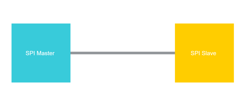
The Serial Peripheral Interface, also commonly referred to as the SPI bus, is a serial, synchronous communication interface that enables data transfer in full duplex mode between devices organized in a Master-Slave architecture.
When it comes to communication among connected devices, data is converted into a series of binary digits (bits) which are represented by electrical signals or voltage levels. Bits are transmitted between devices through various methods, depending on the communication protocol and the specific hardware being used. Regarding the SPI communication protocol, bits are transmitted over dedicated communication lines or channels, following the rules and specifications of the chosen communication protocol. This is typically called full-duplex communication mode and is commonly used in scenarios that require immediate bidirectional data exchange.
The 4-wire configuration
To understand all the essential aspects of the SPI protocol, let us consider the simplest configuration, where one Master and one Slave are connected together.
In this case, the SPI (often referred to as a 4-wire bus) is going to use four dedicated lines:
- Master Output Slave Input (also referred to as MOSI)
- Master Input Slave Output (or MISO)
- Serial Clock (shortened as SCLK)
- Chip Select (CS or also known as Slave Select, SS)
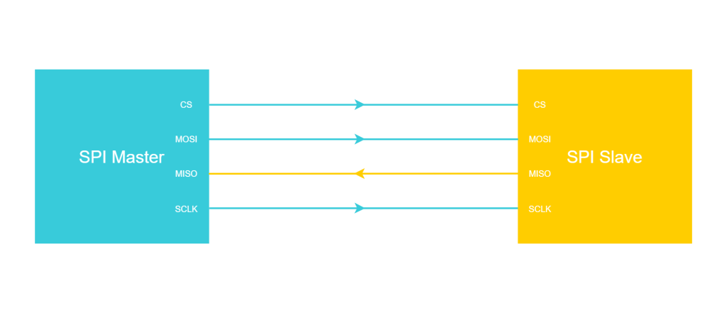
At the beginning of an SPI transaction, the Master pulls low the Chip Select line associated with the addressed slave. In our specific example, there is just one Slave and consequently, only one Chip Select. At this point, the Master provides a Clock Signal sent over the SCLK line. The number of clock pulses will be equal to the number of bits that are going to be exchanged. Note that SPI communication operates with one Master and multiple Slave topology and only the Master is responsible for generating a Clock Signal.
In general, the data is organized in words of a typical size of 8, 16, or 32 bits, and in a single transaction, the SPI will be able to exchange one or multiple words. For example, If the word size is 16 bits, the SPI transaction can be any multiple of 16 bits in length, such as 16, 32, 48, and so on.
If we would have a transaction of 8 bits, we would have 8 clock cycles and for each cycle, a bit going from Master to Slave on the MOSI line and a bit going from Slave to Master over the MISO line.
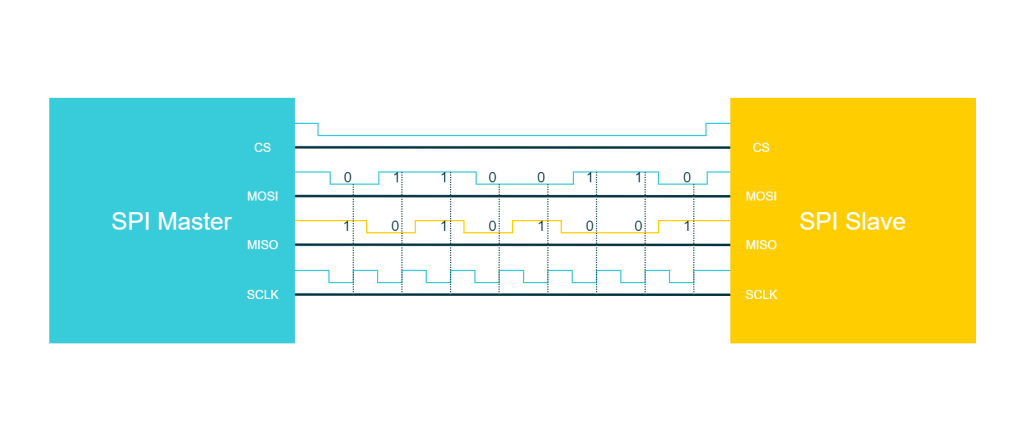
As there is a dedicated line synchronizing the communication (i.e. the clock line), the SPI protocol is said to be a synchronous communication. Multiple bits are transmitted over the same line with proper timing and this makes it a serial protocol. Finally, dedicated lines are employed to communicate simultaneously in both directions (i.e. MOSI and MISO) and this makes it a full duplex protocol.
SPI line directionality: push-pull vs. open-drain
After selecting the SPI topology, the directionality of the communication lines is automatically determined as shown in the table below:
| PIN | MASTER PERSPECTIVE | SLAVE PERSPECTIVE |
|---|---|---|
| SCLK | Out | In |
| CS | Out | In |
| MOSI | Out | In |
| MISO | In | Out |
Since directionality remains fixed over time, SPI pins operate in push-pull mode. This refers to the pins being capable of driving high and low the line. There are some other protocols, when data flows on a line bidirectionally. For example, it is the case of the I2C, where following a specific protocol Master and Slave content the data line. In this case, if for some reason Master and Slave try to pull up and low contemporaneously the line we would have a short circuit. Conversely to the SPI, the I2C requires lines to operate in open-drain mode. For a better understanding between push-pull and open-drain you may want to have a look at the article Fundamentals of Digital Circuitry.
The clock signal
The clock signal is a periodic signal generated by the Master over the SCLK line to synchronize the data transmission. Generally, the Master device is typically a microcontroller, while the Slave is usually a peripheral such as an accelerometer. However, it’s important to note that this is not an absolute rule, as any device capable of generating and controlling the Clock Signal can be designated as the Master in the SPI protocol.
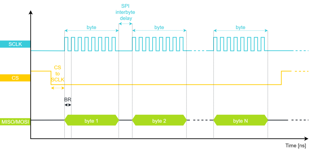
Unlike certain other communication protocols, SPI does not utilize framing bits or start/stop bits. Therefore, for each clock cycle, a bit is transmitted and a bit is received. For this reason, often the SPI clock speed is referred to as the baud rate. In general, the SPI Master has the chance to choose in-between a wide range of clock speeds. However, SPI Slaves are typically cost-effective devices with a limited range of speed. Therefore, it is the Master that has to adapt to the Slave.
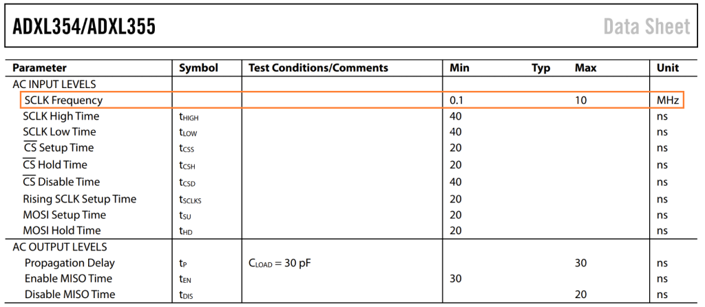
For example, the ADXL355 is an accelerometer behaving as an SPI Slave. Its datasheet specifies a maximum frequency of 10MHz that cannot be exceeded. This ensures that the ADXL355 has enough time to process the incoming data and prepare an answer in a timely manner.
Theoretically, the SPI has no overhead, and increasing the clock speed would directly increase the transfer rate. The SPI was designed for high scalability, this means that by increasing the clock speed, the data transfer rate can reach hundreds of megabits per second or even more. It is important to notice, that when the clock speed is close to gigahertz the lines start to behave as transmission lines and the parasitic parameters can deteriorate the signal integrity to the point the communication is no longer reliable.
However, it’s important to note that there is always some level of overhead present in SPI communication. This is caused by factors such as the time between activating the Chip Select and the first clock edge, as well as potential delays between bytes of data. These factors introduce additional delay which can affect the effective data rate.
SPI modes
The SPI comes with four configurations of the clock signal that the Master can use. However, SPI Slaves are typically cost-effective devices designed to operate in only one of those modes. When interfacing with a Slave for the first time, one of the initial tasks is to determine the accepted maximum baud rate and clock signal mode, often by referring to its datasheet.
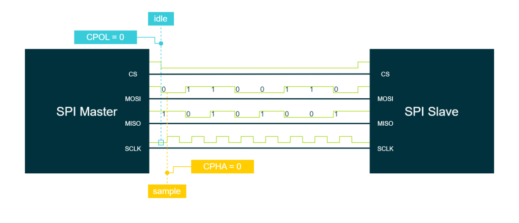
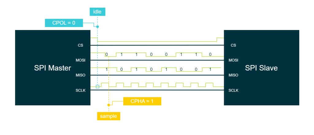
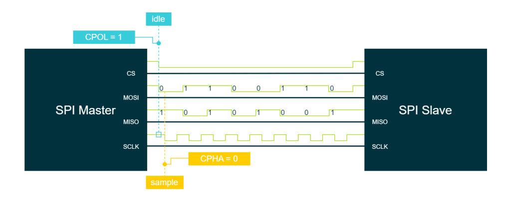
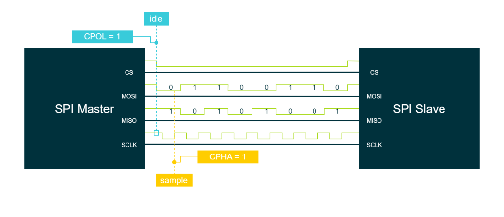
The four SPI modes are achieved by combining two properties of the clock signal: clock polarity (CPOL) and clock phase (CPHA). Their combination determines which edge of the Clock Signal is used to drive and sample data signals.
CPOL can be set to either low (typically represented with 0) or high (typically 1), and it determines the clock level in the idle state (i.e. when the SPI is not transmitting). CPHA is needed to determine whether the data sampling and transmission occurs on the first edge of the clock (typically represented with 0) or the second edge (typically 1). The following table represents the four possible combinations of CPOL and CPHA often referred to as SPI modes:
| SPI MODE | CPOL | CPHA |
|---|---|---|
| 0 | 0 | 0 |
| 1 | 0 | 1 |
| 2 | 1 | 0 |
| 3 | 1 | 1 |
The modes often create confusion because they are explained in terms of “sampling” and “shifting out”. In an SPI communication, the Master and Slave must prepare and sample a bit per clock cycle. To avoid issues, the bit needs to be prepared in advance. Sampling refers to the moment when data is captured from the communication line (i.e. the MISO line for the master and the MOSI line for the slave). This sampling moment aligns with a clock edge, requiring the data to be prepared at the preceding clock edge. For instance, if the Master samples data on the falling clock edge, the Slave must shift it out on the preceding rising edge.
From here and out, we are going to focus only on the sampling edge. So for example, if CPOL and CPHA are both 0 (condition defined as Mode 0) the CLock Signal starts with a low state, and the data is sampled on the first edge which happens to be the rising edge.
When CPOL is set to 0 and CPHA is 1 (Mode 1) the clock signal starts with a low state, and the data is sampled on the second edge which happens to be the falling edge.
In Mode 2 of the SPI communication protocol, where CPOL is 1 and CPHA is 0, the clock signal starts in a high state, and the data is sampled on the first edge of the clock signal which happens to be the falling edge.
In Mode 3 of SPI communication, when both CPOL and CPHA are set to 1, the clock signal starts in a high state, and the data is sampled on the second edge of the clock signal which happens to be the rising edge.
To better understand SPI modes it’s useful to examine an example. Let’s consider the Analog Devices ADXL355 being our SPI Slave. This device operates in Mode 0 (clock polarity CPOL = 0 and the clock phase CPHA = 0). Looking at the datasheet of this device, we can find out the modes clearly stated in words. However, this is not always the case for SPI slaves. An important skill is to being able to determine the modes by simply looking at the timing diagram.
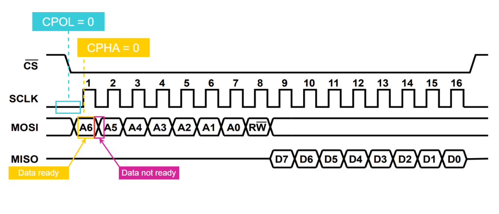
The picture above shows the timing diagram of a single-byte write and single-byte read operation for the ADXL355. From this, we can observe several important things. Firstly, the clock lies in a low state at the beginning of the communication which brings us to deduce that the CPOL is 0.
If we look at the MOSI line, as an example focusing on the A6 bit we can notice a cross-shape symbol that indicates the line may commute during that time, hence it has not a determined value (data not prepared yet). After some time, the line either assumes a high value or a low value and keeps so until the next transition (data ready). To understand the clock phase we need to check if the data is ready on the first or on the second clock edge. Back to the timing diagram, the bit A6 like any other else is ready on the first clock edge which brings us to deduce that CPHA is 0.
Chip Select
The chip select signal serves as a control mechanism to choose the specific slave device with which the master intends to establish communication. Data transfer begins when the master device lowers the CS. It is an active-low signal, meaning that it is held high when not in use and pulled low when the specific peripheral needs to be selected. When this happens, the communication starts and the master and slave start transmitting and receiving data simultaneously over MISO and MOSI lines.
It should be noted that when the Chip Select is kept high its MISO, MOSI, and SCLK lines are in a high impedance state to avoid electrical conflicts on the lines.
In embedded systems, the SPI communication protocol can be employed in two different topologies: the choice lies in between the Independent Mode and Cooperative Mode, also known as Daisy Chain.
Independent mode
In the Independent Mode, each Slave has its own dedicated CS line. The Master lowers one CS at a time to choose with which Slave to communicate. In this configuration, we would have Slaves and Master sharing the SCLK, MOSI, and MISO lines. In this topology, the Master can address independently each Slave which is the reason why it is called Independent Mode.
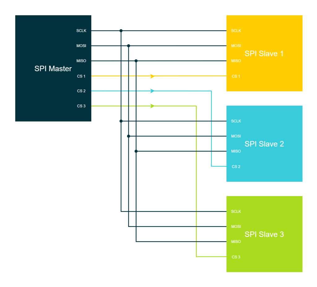
It is important to notice that the Master will be time divided between Slaves. However, having the chance to address each device independently the time division can be kept flexible. On the other hand, this topology requires a large number of lines (3 + Number of Slaves).
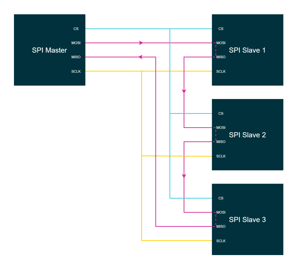
Cooperative mode
In this configuration, all the Slaves shared the SCLK and the CS with the Master. Meanwhile, from the data line point of view, the devices will be chained. The output of the Master (MOSI) goes into the input of the first Slave (MISO). The output of the first Slave (MISO of Slave1) goes into the input of the next Slave (MOSI of Slave2). This scheme continues until the last Slave in the chain closes on the Master. For this reason, this topology is often called Daisy-Chain.
This topology limits the number of lines back to four compromising flexibility in the time partitioning of the Master. Indeed, the idea behind this topology is that the devices behave like a long-shift register. To address the last device in the chain, we need to shift through the entire chain.
To give an example, let us consider a Daisy-Chain of three Slaves and a data frame of 16 bits. If we were to communicate with the third Slave of the chain we would need to exchange 48 bits to reach the last device (3 multiplied by 16 bits). This is because the data needs to be sequentially shifted through the first and second Slaves before reaching the third one.
In this scenario, we need to address each device in the chain that lies before the one with which we actually want to communicate. This limits our options when deciding how to manage the Time Division Scheme of the Master. Additionally, it should be noted that not all the SPI are compliant to operate with a Daisy-Chain topology.
Conclusion
In summary, the SPI communication protocol offers a versatile solution for data exchange between devices. The 4-wire connections, consisting of MISO, MOSI, CS, and clock, enable simultaneous transmission and reception of data sent one bit at a time. The clock modes determine the timing and synchronization of data transmission and the chip select allows the master to specifically select the slave to communicate with. The data frame is mainly made of 8 bits whose interpretation and the logic implemented depend on the devices involved in the communication.
Overall SPI protocol provides a reliable and flexible means of communication. By leveraging its capabilities and understanding the nuances of clock modes, chip select configurations, and pin dynamics, developers can effectively harness the potential of the SPI protocol for diverse embedded systems and communication scenarios.
Great article just what the doctor ordered