
Using STM32 ADC with ChibiOS ADC Driver
Important notice
Please note that the information contained in this article may no longer be accurate or useful due to changes in the ChibiOS codebase and ChibiStudio.
Unfortunately, at the moment there is no direct replacement for this article. However, we are in the process of rewriting the series with updated information, a better writing style, and improved ease of use. The new series will also be completed with a larger set of examples and exercises to help you better understand how to use ChibiOS and ChibiStudio.
We welcome any feedback or suggestions you may have, so please don’t hesitate to get in touch with us.
Thank you for your interest in our content.
Why a converter
A microcontroller is a system which works on bits and bitstreams more than analog signals, anyway, those signals are still widely used in many fields especially in audio and power applications. An Analog to Digital Converter (or ADC) is a system that converts such kind of signals in a sequence of discrete values directly interpretable by the microcontroller. Such kind of converter is widely used in embedded systems to deal with those peripherals which work with analog signals like potentiometers, analog microphones or sensors.
Some examples?
- Analog sensors which produce a voltage level proportional to the measured property, like industrial temperature sensor which usually are made with a calibrated Diode.
- A 2-axis joystick you probably have seen on the PlayStation controller. Each axis is actually a potentiometer and it is possible to read it using two channels of the STM32 ADC. We wrote an article about that.
- The guitar pickups are actually a pressure sensor which is able to convert air pressure variation produced by chords vibration into an electric signal.
Once a signal has been sampled with an ADC, it is possible to manipulate it digitally. Considering the guitar pickup example, after the conversion, it is possible to use the microcontroller to apply digital sound effects, for example, equipping the guitar with a small PCB which mounts a micro and few electronics. Cool right? Yeah, and the coolest part is that someone created a prototype base on this idea (take a look if you want).
The Analog to Digital Convert
The theory related to the ADC is particularly large and there is a lot of literature about this topic. The converters are indeed largely used in many fields which go from the Laboratory Test Equipment to Microelectromechanical systems. Because of that, there are many implementation and variants of them to match all the different needs. In this chapter, we would just explain a few concepts you should know to deal with ADC.
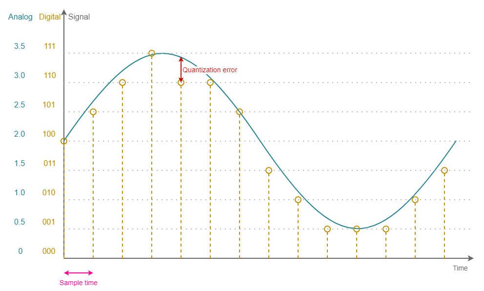
An ADC converts an analog continuous-time signal in a digital discrete-time signal. For example, in the next figure, we can spot a time continuous analog sinusoid in blue and the digital version of the same signal in orange.
Resolution
The first notion we want to introduce here is the Resolution which represents the number of discrete values that the ADC can produce. The sampled values are stored as binary code, a power of 2, and the ADC resolution is often expressed in bits more than in absolute value. In the previous example the ADC was able to produce up to 8 different value (from 0 to 7 or in binary from 0b0 to 0b111): in such case, we can state that this ADC has a 3-bit resolution.
Extending this notion, an ADC having a resolution in bit equal to n will generate sampled values in the range

Full-scale voltage range
An ADC is able to sample only voltages in a specific range. Usually, ADC is able to convert only signals which go from reference ground to a maximum positive value which is known as Full-scale voltage range (or even FSR). Anyway, a more general definition of full scale range would be

To avoid sensitivity reduction as well as distortion or noise introduction, the input of an ADC is a clean conductor with no protection diodes nor conditioning circuitry and this means that user shall pay attention to provide signals which amplitude is coerced in the proper range. To measure signals which are out of range indeed the signal shall be usually conditioned by external circuitry. An example of conditioning circuitry is that used in the vertical channels of oscilloscopes which are even configurable allowing to select between Alternate and Direct Coupling as well as tune the FSR.
Back to the previous example, the value 0b111 correspond to a 3.5V input and 0b0 to 0V. Thus we can state the ADC has a full-scale range of 3.5V.
Voltage resolution
While the FSR represent the range of input voltage, the Resolution represents the range in which lays the output binary code. The ratio of these two quantities provides useful information about the “weight” of the LSb of the output binary value in term of voltage. This new quantity is known as Voltage resolution

Considering the previous example, the voltage resolution is

Quantization error
As seen in the previous example, the LSb of the binary code has a value of a half volt. This means we will not see any output variation if the input is 0.5V or 0.9V: both will be converted as 0b001.
Converting a continuous quantity in a discrete one, there is always an information loss. Such loss is much greater the smallest is the resolution of our ADC. The quantization error can be evaluated by computing the difference between an input value and its quantized value. In the previous figure, we have marked the quantization error for the 5th sample which is marked by a dark red arrow. Here the error is very evident but you should keep in mind that there always is a quantization error: in some cases, it is very small, almost negligible. Anyway, it is clear the quantization error has an upper bound which is actually the voltage resolution
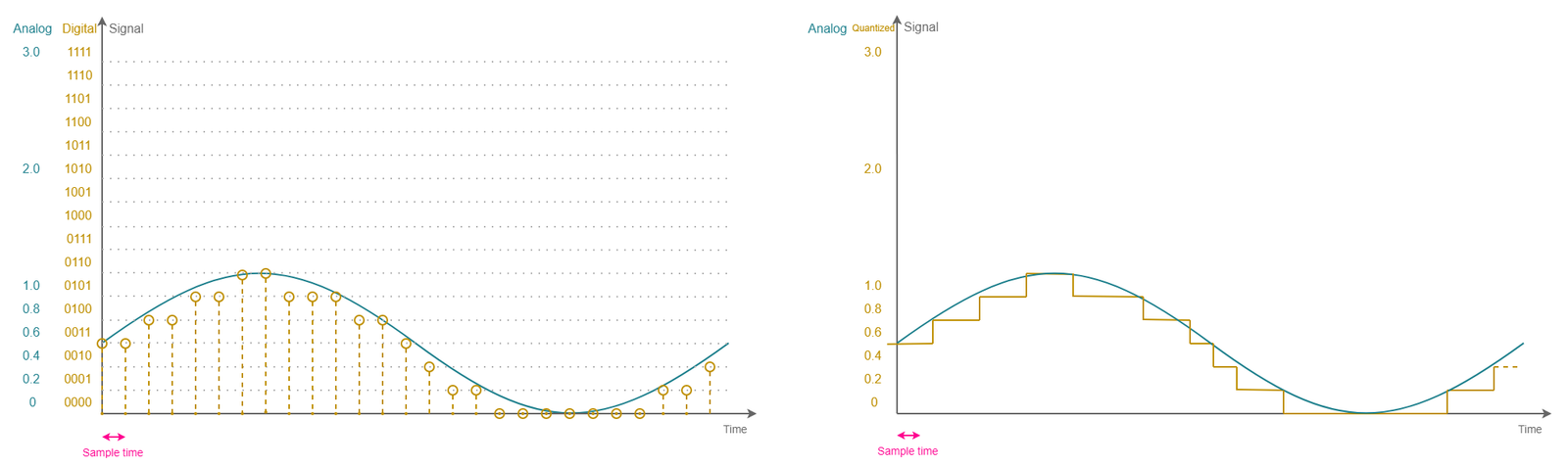
There a couple of action we can take to reduce the quantization error side effect: one is to reduce the voltage resolution which means to have a higher resolution, the other is to exploit the whole conversion range sampling wide signals which overlap the range as much as possible. Let us clarify this with an example considering a 4-bit ADC with an FSR of 3.0V. In such
case we have

Let us now consider that our input is a signal in range 0-1.2V. In such scenario we are not using the whole input range and we are using more or less only 3-bits as

and the next figure shows which would be the effect of quantization on the sampled waveform
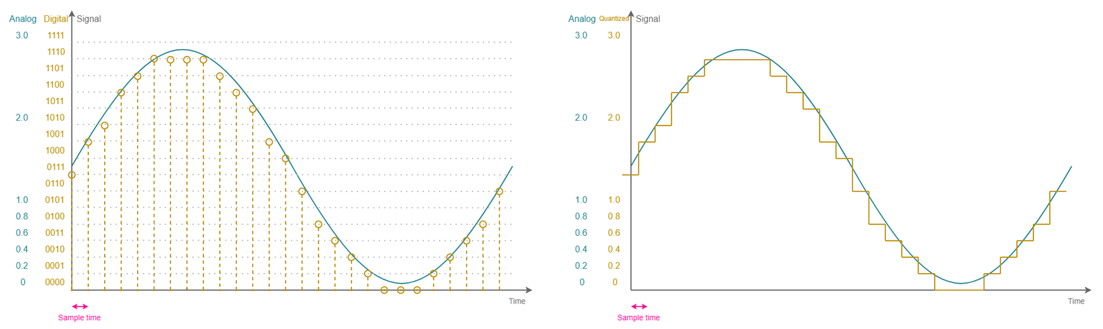
If we amplify the input signal with an external circuitry trying to overlap the whole input range we would make better use of our digital representation space. Indeed, in such case, we will use all the 16 symbols (instead of only 7) to represent the sampled version of our signal. The next figure shows the result of such operation: we can see the quantization error is still there but we have a lower information loss.
If the quantization error is still too big for our application another solution could be to increase the representation space of our digital output or in other words to use an ADC having a better resolution.
Sampling rate
The ADC samples the signal each while. Usually, the time elapsed between two samples remains constant in time and takes the name of Sampling time or, considering its reciprocal, we have a frequency named Sampling Rate. In our example, the sampling time is represented by the pink arrow. Note that usually sampling frequency is measured as Samples per second (S/s) and multiples (kS/s, MS/S or GS/s).
In certain cases having a constant sampling cadence over time is a requirement of the application and in those scenarios, the ADC is usually triggered by an external entity which ensures a proper timing (for example a hardware timer). An example of an application which requires such precision is audio sampling whereas you often would convert an analog audio signal in a Waveform Audio File Format (or .wav) which is usually a PCM having a constant bitrate (usually 44.1kHz, 48kHz or 96kHz).
Note that maximum sampling rate sets a constraint on input signal maximum frequency we are able to perceive: we are blind on frequencies greater than half of the sampling frequency as Nyquist states.
The STM32 ADC peripheral
The working principle of a SAR ADC
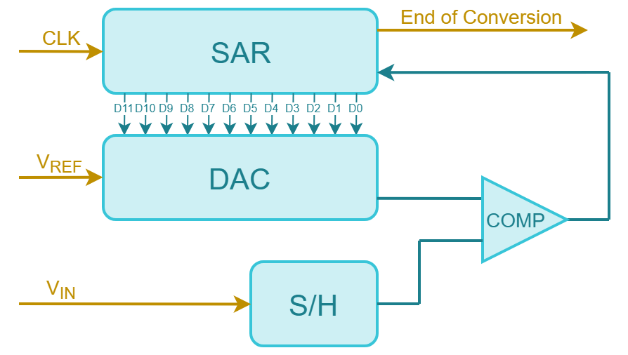
Every STM32 equips a 12-bit resolution Successive Approximation ADC. In figure 4 we can see a principle diagram of such ADC. In the scheme we can spot:
- A Sample and Hold circuit which samples the input voltage and keep it unchanged until the end of conversion. This circuit requires a certain Sampling Time usually expressed in clock cycles to do its job.
- A Digital to Analog Converter which purpose is to convert a binary code into a voltage (its behavior is the dual of the ADC).
- A Comparator which purpose is to compare its inputs. The result of a comparison is a logic level that indicates if the DAC output is greater or smaller than S/H output.
- The Successive Approximation Register which is a complex logic which scope is to provide an approximated binary code to the DAC and, when the conversion is over, the output of conversion.
The conversion happens as follows:
- The input is sampled in m clock cycles by the sample and hold.
- The SAR set the bit D11 to ‘1’
- The DAC receives thus 0b1000 0000 0000 generating an output voltage
- The comparator compares its two inputs. If the S/H output is greater than the DAC output the D11 remains to ‘1’ otherwise it is changed to ‘0’
- The SAR set the bit D10 to ‘1’ while D11 depends on the previous cycle.
- The DAC receives a new value which better approximate the input generating a new output voltage
- The comparator compares its two input. If the S/H output is greater than the DAC output the D10 remains to ‘1’ otherwise it is changed to ‘0’
- …. the loop continues on remaining bits
When all the bit have been processed the SAR contains a bit code which better approximate the input value. Note that each bit of the SAR requires is determined in a clock cycle, thus the total time required by SAR to perform a conversion is equal to the resolution of the ADC expressed in bits. The total number of clock cycles required is thus

Multiplexed input and sequences
Each STM32 ADC has many input sources usually named channel, anyway, the ADC can sample one channel at a time thus the channels are multiplexed. These channels are identified with a progressive number starting from 0, the first 16 channels are usually assigned to external sources (e.g. are connectable to the outside world through the GPIO peripheral). Other channels are internal sources like the VBAT (e.g. the voltage of the backup battery usually used to keep up the Real Time Clock) or like the VTEMP (e.g. the voltage of internal temperature sensor).
External inputs are assigned to some specific GPIO which shall be configured in Analog Mode to ensure the proper connection with the ADC. You can find information about these assignments exploring the Datasheet of the STM32 and you should also take a look at the article Using STM32’s GPIO with ChibiOS’ PAL Driver if you didn’t.
To guarantee flexibility the ADC is able to convert also a group of channels organized is a user-defined sequence. The sequence can be configured acting on some registers known as ADC Sequence Registers. Usually, those registers are three (ADCx_SQR1, ADCx_SQR2, and ADCx_SQR3) and the maximum sequence length is 16 anyway this can vary across different microcontroller even if working principle remains quite the same. Each sequence register is split in many bit fields representing an element of the sequence and in the first register, there is also a bit field representing the length of the whole sequence (actually length minus one, for instance, if we store 3 in it we are stating the whole sequence length is 4).
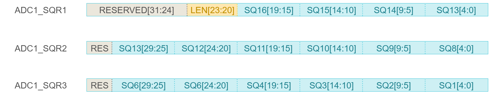
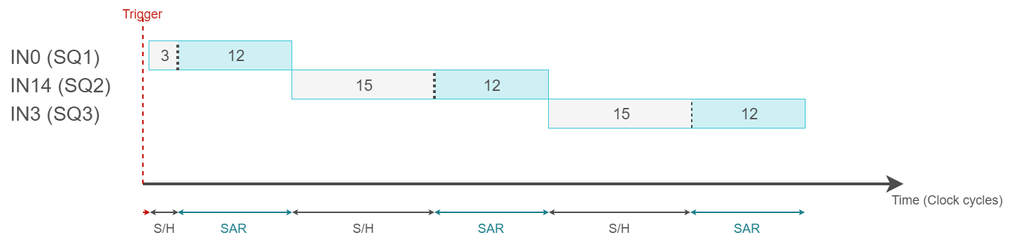
The sequence can be composed in a completely arbitrary way and the user can even repeat the same channel more than once. To configure it we have to populate these bitfields with the numeric identifier of the channel. Thus, if we would set a sequence like ADC_CHANNEL_IN0, ADC_CHANNEL_IN14 and ADC_CHANNEL_IN3 we should set
/* Len bitfield set as n - 1 (2 in this case) as specified by RM. */
ADC1_SQR1 = (3 - 1) << 20; /* 0x200000 */

/* No element in this register */
ADC1_SQR2 = 0;


/* SQ1 bit field set as 0, SQ2 as 14 and SQ3 as 3 */
ADC1_SQR3 = (3 << 10) | (14 << 5) | (0 << 0); /* 0xDC0 */
If you are not familiar with shift and bitwise operators you should definitely read Registers and bit masks which is a short article that explains how to deal with read-modify-write paradigm and registers in general.
We will see later that ChibiOS ADC driver exposes some helper macros and constants to compose the sequence registers.
Sampling time and trigger
The ADC requires to be triggered to start a conversion.
Once triggered the STM32 ADC will sample the whole sequence converting subsequently all the channel of the sequence at the maximum rate.
This means there is no pause between the conversion of one channel and the next one in the sequence. We can anyway influence the sampling time of the whole sequence acting on the sampling time of each sequence element. This can be done basically through two parameters:
- The ADC resolution which can be configured through one of its control register (usually ADCx_CR1). Note that available resolutions are limited (usually 6-bit, 8-bit, 10-bit or 12-bit);
- The ADC S/H circuit sample time which can be configured independently on each channel acting on some registers (usually 2) known as ADC Sample Rate Register (ADCx_SMPR1 and ADCx_SMPR2)
Sample rate registers are split into many bit fields each one representing the sampling rate of a channel (SMP0 is the rate of ADC_CHANNEL_IN0, SMP1 of ADC_CHANNEL_IN1, and so on).
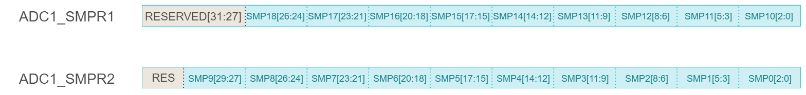
The available sample rate values are limited and possible values depend on specific driver version (for example 3, 15, 28, 56 cycles). The total sample time of each channel can be computed with the next formula
The sample time of the whole sequence is the sum of the time required to sample each channel. As instance let us assume that
- the sequence is again ADC_CHANNEL_IN0, ADC_CHANNEL_IN14, and ADC_CHANNEL_IN3
- ADC resolution is 12-bit
- the sample rate for ADC_CHANNEL_IN0 is 3 cycle
- the sample rate for ADC_CHANNEL_IN14 is 15 cycle
- the sample rate for ADC_CHANNEL_IN3 is 15 cycle
In such scenario the number of clock cycles will be 3 + 12 + 15 + 12 + 15 + 12 (plus a fraction of a clock cycle due to an eventual misalignment between ADC clock and trigger).
The STM32 ADC can be triggered in Software by writing a trigger bit in a control register (usually the SWSTART bit in the ADCx_CR2). It can also be triggered by an external signal which can be injected by the outside world or generated by an internal timer: this option is largely used when sampling shall be performed with precise timing. For this purpose, there are certain General Purpose Timer of the STM32 which have no output channel but only internal lines just to be used as a trigger for the ADC and DAC peripherals: such timers are usually the TIM6 and TIM7.
The behavior of the trigger depends on the Conversion Mode of the ADC. If the ADC is configured as Single Conversion Mode (on trigger event) it converts a sequence then stops. If it is configured in Continuous Conversion Mode the ADC starts a new conversion as soon as it finishes one.
The ChibiOS ADC driver
The ChibiOS ADC driver exploits all the feature of the STM32 ADC to cover a large number of scenarios offering both blocking and non-blocking functions, fully configurable sample groups, circular/linear conversion modes, and configurable trigger.
Each API of the ADC Driver starts with the prefix “adc”. Function names are camel-case, pre-processor constants uppercase and variables lowercase.
Different driver same approach
Comparing the ADC driver with previously presented Serial Driver we can notice that there are some certitudes in ChibiOS: one of these is for sure the consistency of design patterns. The ADC driver is organized like every other simple driver of ChibiOS\HAL:
- The whole driver subsystem can be enabled disabled through the proper switch in the halconf.h. The switch name is HAL_USE_ADC.
- To use the driver we have then to assign it an ADC peripheral acting on mcuconf.h.
- Assigning a peripheral to the driver a new object will become available: ADCD1 on ADC 1 assignation, ADCD2 on ADC 2 and so on.
- Each ADCDx object represents a driver which implements a Finite State Machine.
- A driver to be used shall be initialized but this is done automatically on halInit();
- Each driver operation (e.g. a conversion) can be done only if the driver has been properly started. This requires a call to adcStart().
- The adcStart() receives as usual two parameters: a pointer to the driver and a pointer to its configuration.
- If the driver is not used it can be stopped through the adcStop().
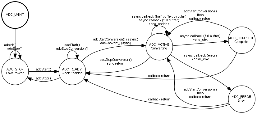
The following figure is the state machine of the driver.
Conversion functions
The ADC driver offers both synchronous and asynchronous conversion function. We already introduced these concepts but let me recall them.
A blocking function blocks the execution of the calling thread until the operation is completed. If the function has some internal wait they are not polled, instead, the calling thread is suspended and the RTOS executes other threads. Such functions are also known as synchronous functions as the calling thread remains in sync with the operation.
A non-blocking function launches the operation and returns to the calling thread which continues to be executed. Such operation is executed in the background, usually in hardware, launching an interrupt on operation complete event. Such IRQ usually is exposed by driver API in the form of a callback. Such functions are also known as asynchronous functions.
The synchronous version of the ADC conversion is the adcConvert
/**
 * @brief   Performs an ADC conversion.
 * @details Performs a synchronous conversion operation.
 * @note    The buffer is organized as a matrix of M*N elements where M is the
 *          channels number configured into the conversion group and N is the
 *          buffer depth. The samples are sequentially written into the buffer
 *          with no gaps.
 *
 * @param[in] adcp      pointer to the @p ADCDriver object
 * @param[in] grpp      pointer to a @p ADCConversionGroup object
 * @param[out] samples  pointer to the samples buffer
 * @param[in] depth     buffer depth (matrix rows number). The buffer depth
 *                      must be one or an even number.
 * @return              The operation result.
 * @retval MSG_OK       Conversion finished.
 * @retval MSG_RESET    The conversion has been stopped using
 *                      @p acdStopConversion() or @p acdStopConversionI(),
 *                      the result buffer may contain incorrect data.
 * @retval MSG_TIMEOUT  The conversion has been stopped because an hardware
 *                      error.
 *
 * @api
 */
msg_t adcConvert(ADCDriver *adcp,
                 const ADCConversionGroup *grpp,
                 adcsample_t *samples,
                 size_t depth) {
  ...
}
the asynchronous one the adcStartConvert
/**
 * @brief   Starts an ADC conversion.
 * @details Starts an asynchronous conversion operation.
 * @note    The buffer is organized as a matrix of M*N elements where M is the
 *          channels number configured into the conversion group and N is the
 *          buffer depth. The samples are sequentially written into the buffer
 *          with no gaps.
 *
 * @param[in] adcp      pointer to the @p ADCDriver object
 * @param[in] grpp      pointer to a @p ADCConversionGroup object
 * @param[out] samples  pointer to the samples buffer
 * @param[in] depth     buffer depth (matrix rows number). The buffer depth
 *                      must be one or an even number.
 *
 * @api
 */
void adcStartConversion(ADCDriver *adcp,
                        const ADCConversionGroup *grpp,
                        adcsample_t *samples,
                        size_t depth) {
  ...
}
Both the conversion functions receive the same parameters. Let us take an overview of them:
The first parameter is, as usual, a pointer to the driver. Remember that the driver shall be already started and configured through the adcStart before to call a conversion function: this is a common pattern in ChibiOS which I use to call start-do-stop.
Anyway, ADC configuration itself is very poor and, in certain driver version, is even empty. This would sound quite strange (especially because we have spent a whole chapter talking about features and configuration of STM32 ADC). This takes us to the second parameter: the ADCConversionGroup. Most of the ADC configuration is indeed demanded to the conversion functions and it is confined in this configuration structure. The logical motivation of this design is that configurations like trigger source, sequence or sample rate are related to the conversion more than to the driver itself.
The ADCConversionGroup contains all the configuration related to the conversion group like the trigger source, the sequence, the sample rate and the conversion mode.
Let me now jump to the fourth parameter which is named depth. The conversion function allows to sample the same conversion group more than once and depth represent the number of times we want to sample the conversion group. Thus if we consider the conversion group length (M) the first dimension we should consider the depth (N) the second.
Thus a conversion function needs a buffer which is actually a matrix M by N which lead us to the third parameter which is actually a pointer to that buffer. The user shall guarantee that the buffer is properly sized to avoid overflow. Note that the sample buffer type is specific of ChibiOS and this allows abstraction on Hardware differences. In this case, adcsample_t is a 16-bit unsigned integer. The data alignment depends on certain configuration we can provide through the ADCConversionGroup.
There are some restrictions about depth: it shall be at least one and it shall be an even number. The first one is almost obvious but to understand the second we should understand how asynchronous conversion works. When we launch the adcStartConvert we have also to provide a callback through the ADCConversionGroup. This callback is also known as end callback (end_cb) and is called in twice specific moments of the conversion:
- when the ADC has filled the first half buffer
- when the ADC has filled the whole buffer.
This is very useful in the circular mode when the conversion continues indefinitely and the matrix is used as a circular buffer. Let us clarify this considering a scenario in which:
- the sequence is ADC_CHANNEL_IN0, ADC_CHANNEL_IN14, and ADC_CHANNEL_IN3,
- conversion depth is 10,
- timing is the same as the previous example,
- conversion is asynchronous (e.g. we have used the adcStartConvert),
- the trigger is software (e.g. conversion starts on adcStartConvert)
In such a scenario, the buffer is a 3×10 matrix. On the call, the adcStartConvert configures the ADC triggering the conversion and promptly returns to calling thread which continues its execution. From here and out, while the kernel is executing threads, the ADC is converting continuously relying on DMA to fill memory with converted data: this means the only way to get in sync with conversion is to use the end callback. As said this callback will be triggered when ADC (more precisely DMA) has filled the first half buffer: in this case, the ADC has performed 5 conversions and it is going to fill the second half buffer: through the callback when the ADC is doing that we can operate on the first half. Next callback will be on the completion of second-half buffer conversion: here the ADC will start to convert overwriting the first half buffer and we can operate on the second one. This solution allows us to operate in real time on sampled data as long as our operations inside the callback are faster the ADC half buffer conversion.
Note that in case of linear conversion callback is triggered only at the end of the whole conversion. Note also that such kind of callback receives certain parameter like a pointer to the driver, a pointer to the buffer currently filled and the size of the converted buffer: this means in circular mode we will receive a pointer to the current half buffer and NxM/2 as size, in case of linear mode we will receive the pointer to the whole buffer and N by M as size.
Back to the circular buffer scenario, it is clear that API requires an additional function to stop the ongoing conversion which could potentially last indefinitely. Such function is the adcStopConversion
/**
 * @brief   Stops an ongoing conversion.
 * @details This function stops the currently ongoing conversion and returns
 *          the driver in the @p ADC_READY state. If there was no conversion
 *          being processed then the function does nothing.
 *
 * @param[in] adcp      pointer to the @p ADCDriver object
 *
 * @api
 */
void adcStopConversion(ADCDriver *adcp) {
  ...
}
Conversion Group configuration
At the end of the day, the most difficult part in ADC usage is to properly configure the conversion group. This is particularly tricky because STM32 ADC has many variants depending on sub-family and in a certain case on specific Microcontroller. ChibiOS\HAL implements many different versions of this driver to resolve hardware differences. Details related to ChibiOS\HAL design can be found in this article.
Currently, there are 4 different drivers version plus a couple of specific ADC driver implementation to cover all the hardware differences across the STM32 subfamilies. From the user point of view, a different driver implementation means different ADC register organizations, different bit mask. By the way, remember that all the hardware differences are confined in configuration structures. In this case, you will have different ADCConversionGroup and ADCConfig while the ADC API itself remains constant.
In what follow we are going to take a deep look in the ADCConversionGroup of the drivers ADCv2 which supports the STM32 “advanced” ADC found on F2, F4, and F7 sub-families. This walkthrough, the testhal demos, and the STM32 reference manual should be far enough to understand how to use other driver versions also.
The first step is to identify which driver version is the proper one for you STM32. In case you want to learn how to do take a look here, otherwise for a quick reference:
- STM32F0xx and STM32L0xx use ADCv1;
- STM32F1xx uses a platform-specific ADC driver;
- STM32F2xx, STM32F4xx and STM32F7xx use ADCv2;
- STM32F3xx and STM32L4xx use ADCv3;
- STM32F37x and STM32F38x use a platform-specific ADC driver;
- STM32H7xx uses ADCv4.
Now, the easiest way to use ADC is to copy some snippets of code from a testhal demo. Such demos are under the folder [chibios_root]\testhal\STM32. In such directory, you can find demos for many every STM32 subfamily. Anyway, it is not guaranteed that you will find runs on your development board.
For example, let us consider the STM32F4 sub-family: reading the readme.txt of the demo [chibios_root]\testhal\STM32\STM32F4xx\ADC we would notice that this demo has been created for STM32F4 Discovery thus will not run on an STM32 Nucleo-64 F401RE. Nevertheless, the ADCConversionGroup used in this demo is compliant with any STM32F4 MCU as well as with STM32F2xx and STM32F7xx families. Thus steps to port this demo are:
- Clone the default demo for STM32 Nucleo-64 F401RE;
- Enable the ADC driver (halconf.h) and assign a peripheral to it (mcuconf.h);
- Copy from the testhal demo the whole main or snippet of code related to ADC.
- Resolve eventual differences like a different identifier of LED line.
Usually, the demos have more than a configuration: this allows the user to make a comparison and understand how configuration works. Now considering the proposed demo it has a couple of configuration. The first one is the simpler and samples 1 channel linearly triggered by software.
static void adcerrorcallback(ADCDriver *adcp, adcerror_t err) {

  (void)adcp;
  (void)err;
}

/*
 * ADC conversion group.
 * Mode:        Linear buffer, 8 samples of 1 channel, SW triggered.
 * Channels:    IN11.
 */
static const ADCConversionGroup adcgrpcfg1 = {
  FALSE,
  ADC_GRP1_NUM_CHANNELS,
  NULL,
  adcerrorcallback,
  0,                        /* CR1 */
  ADC_CR2_SWSTART,          /* CR2 */
  ADC_SMPR1_SMP_AN11(ADC_SAMPLE_3),
  0,                        /* SMPR2 */
  0,                        /* HTR */
  0,                        /* LTR */
  0,                        /* SQR1 */
  0,                        /* SQR2 */
  ADC_SQR3_SQ1_N(ADC_CHANNEL_IN11)
};
This configuration is extremely simple but has a lot of field many of which are empty. What if the user has to modify this configuration to achieve a custom behavior?
To create some custom configuration, it is required to investigate the meaning of each ADCConversionGroup field taking a look to how the structure is defined in the ChibiOS LLD code. More in detail this structure is defined in the file hal_adc_lld.h and each driver version has its own file. As example the path of LLD header for ADCv2 is [chibios_root]\os\hal\ports\STM32\LLD\ADCv2\hal_adc_lld.h. As counterexample, the one for STM32F37x is [chibios_root]\os\hal\ports\STM32\STM32F37x\hal_adc_lld.h.
Back to ADCv2 we have
/**
 * @brief   Conversion group configuration structure.
 * @details This implementation-dependent structure describes a conversion
 *          operation.
 * @note    The use of this configuration structure requires knowledge of
 *          STM32 ADC cell registers interface, please refer to the STM32
 *          reference manual for details.
 */
typedef struct {
  /**
   * @brief   Enables the circular buffer mode for the group.
   */
  bool                      circular;
  /**
   * @brief   Number of the analog channels belonging to the conversion group.
   */
  adc_channels_num_t        num_channels;
  /**
   * @brief   Callback function associated to the group or @p NULL.
   */
  adccallback_t             end_cb;
  /**
   * @brief   Error callback or @p NULL.
   */
  adcerrorcallback_t        error_cb;
  /* End of the mandatory fields.*/
  /**
   * @brief   ADC CR1 register initialization data.
   * @note    All the required bits must be defined into this field except
   *          @p ADC_CR1_SCAN that is enforced inside the driver.
   */
  uint32_t                  cr1;
  /**
   * @brief   ADC CR2 register initialization data.
   * @note    All the required bits must be defined into this field except
   *          @p ADC_CR2_DMA, @p ADC_CR2_CONT and @p ADC_CR2_ADON that are
   *          enforced inside the driver.
   */
  uint32_t                  cr2;
  /**
   * @brief   ADC SMPR1 register initialization data.
   * @details In this field must be specified the sample times for channels
   *          10...18.
   */
  uint32_t                  smpr1;
  /**
   * @brief   ADC SMPR2 register initialization data.
   * @details In this field must be specified the sample times for channels
   *          0...9.
   */
  uint32_t                  smpr2;
  /**
   * @brief   ADC watchdog high threshold register.
   * @details This field defines the high threshold of the analog watchdog.
   */
  uint16_t                  htr;
  /**
   * @brief   ADC watchdog low threshold register.
   * @details This field defines the low threshold of the analog watchdog.
   */
  uint16_t                  ltr;
  /**
   * @brief   ADC SQR1 register initialization data.
   * @details Conversion group sequence 13...16 + sequence length.
   */
  uint32_t                  sqr1;
  /**
   * @brief   ADC SQR2 register initialization data.
   * @details Conversion group sequence 7...12.
   */
  uint32_t                  sqr2;
  /**
   * @brief   ADC SQR3 register initialization data.
   * @details Conversion group sequence 1...6.
   */
  uint32_t                  sqr3;
} ADCConversionGroup;
The first four fields are common across every driver version:
- circular, is a boolean which programs the ADC to work in the circular mode when true or linear otherwise. In linear mode the ADC converts a group one time than stops; In the circular mode, the ADC converts group continuously using the sample buffer in a circular way.
- num_channels, is an unsigned representing the length of the sequence. This value is used internally to configure the LEN bit field of the ADCx_SQR1 register. Remember that the maximum number depends on hardware as each sequence elements is actually a bit field in the sequence registers.
- end_cb, is that callback, the one executed when the conversion is completed and, in case of a circular buffer, on half buffer.
- error_cb, which is a callback triggered on ADC hardware error.
The other fields are instead hardware dependent and thus can change between different version of the ADC driver. Basically, these fields represent the value of some ADC registers. Some of them can be ignored in most of the scenario and left to zero, others require close attention:
- cr1, cr2, … crx are the control registers. The driver configures them partially but we can use them to change some configuration like ADC resolution, data alignment or trigger source.
- sqr1, sqr2, … sqrx are the sequence registers.
- smpr1, smpr2, … smpr3 are the sample rate registers.
To compose registers value we can use the bitmasks already defined in the CMSIS header files. Such files contain all the definition of every bit field of every register of our MCU. It is possible to find under [chibios_root]\chibios_trunk\os\common\ext\ST\. Each MCU has is own CMSIS header file as the register map changes with a microcontroller. As example the file for the STM32F401RE is [chibios_root]\chibios_trunk\os\common\ext\ST\STM32F4xx\stm32f401xe.h.
What follows is some bit masks definition for the ADC registers. Note that has some ChibiOS drivers already uses those bitmasks internally, the proper file for the micro in use is already included.
/******************************************************************************/
/*                                                                            */
/*                        Analog to Digital Converter                         */
/*                                                                            */
/******************************************************************************/

/********************  Bit definition for ADC_SR register  ********************/
#define ADC_SR_AWD_Pos            (0U)
#define ADC_SR_AWD_Msk            (0x1U << ADC_SR_AWD_Pos)                     /*!< 0x00000001 */
#define ADC_SR_AWD                ADC_SR_AWD_Msk                               /*!<Analog watchdog flag */
#define ADC_SR_EOC_Pos            (1U)
#define ADC_SR_EOC_Msk            (0x1U << ADC_SR_EOC_Pos)                     /*!< 0x00000002 */
#define ADC_SR_EOC                ADC_SR_EOC_Msk                               /*!<End of conversion */
#define ADC_SR_JEOC_Pos           (2U)
#define ADC_SR_JEOC_Msk           (0x1U << ADC_SR_JEOC_Pos)                    /*!< 0x00000004 */
#define ADC_SR_JEOC               ADC_SR_JEOC_Msk                              /*!<Injected channel end of conversion */
#define ADC_SR_JSTRT_Pos          (3U)
#define ADC_SR_JSTRT_Msk          (0x1U << ADC_SR_JSTRT_Pos)                   /*!< 0x00000008 */
#define ADC_SR_JSTRT              ADC_SR_JSTRT_Msk                             /*!<Injected channel Start flag */
#define ADC_SR_STRT_Pos           (4U)
#define ADC_SR_STRT_Msk           (0x1U << ADC_SR_STRT_Pos)                    /*!< 0x00000010 */
#define ADC_SR_STRT               ADC_SR_STRT_Msk                              /*!<Regular channel Start flag */
#define ADC_SR_OVR_Pos            (5U)
#define ADC_SR_OVR_Msk            (0x1U << ADC_SR_OVR_Pos)                     /*!< 0x00000020 */
#define ADC_SR_OVR                ADC_SR_OVR_Msk                               /*!<Overrun flag */

/*******************  Bit definition for ADC_CR1 register  ********************/
#define ADC_CR1_AWDCH_Pos         (0U)
#define ADC_CR1_AWDCH_Msk         (0x1FU << ADC_CR1_AWDCH_Pos)                 /*!< 0x0000001F */
#define ADC_CR1_AWDCH             ADC_CR1_AWDCH_Msk                            /*!<AWDCH[4:0] bits (Analog watchdog channel select bits) */
#define ADC_CR1_AWDCH_0           (0x01U << ADC_CR1_AWDCH_Pos)                 /*!< 0x00000001 */
#define ADC_CR1_AWDCH_1           (0x02U << ADC_CR1_AWDCH_Pos)                 /*!< 0x00000002 */
#define ADC_CR1_AWDCH_2           (0x04U << ADC_CR1_AWDCH_Pos)                 /*!< 0x00000004 */
#define ADC_CR1_AWDCH_3           (0x08U << ADC_CR1_AWDCH_Pos)                 /*!< 0x00000008 */
#define ADC_CR1_AWDCH_4           (0x10U << ADC_CR1_AWDCH_Pos)                 /*!< 0x00000010 */
#define ADC_CR1_EOCIE_Pos         (5U)
#define ADC_CR1_EOCIE_Msk         (0x1U << ADC_CR1_EOCIE_Pos)                  /*!< 0x00000020 */
#define ADC_CR1_EOCIE             ADC_CR1_EOCIE_Msk                            /*!<Interrupt enable for EOC */
#define ADC_CR1_AWDIE_Pos         (6U)
#define ADC_CR1_AWDIE_Msk         (0x1U << ADC_CR1_AWDIE_Pos)                  /*!< 0x00000040 */
#define ADC_CR1_AWDIE             ADC_CR1_AWDIE_Msk                            /*!<AAnalog Watchdog interrupt enable */
#define ADC_CR1_JEOCIE_Pos        (7U)
#define ADC_CR1_JEOCIE_Msk        (0x1U << ADC_CR1_JEOCIE_Pos)                 /*!< 0x00000080 */
#define ADC_CR1_JEOCIE            ADC_CR1_JEOCIE_Msk                           /*!<Interrupt enable for injected channels */
#define ADC_CR1_SCAN_Pos          (8U)
#define ADC_CR1_SCAN_Msk          (0x1U << ADC_CR1_SCAN_Pos)                   /*!< 0x00000100 */
#define ADC_CR1_SCAN              ADC_CR1_SCAN_Msk                             /*!<Scan mode */
#define ADC_CR1_AWDSGL_Pos        (9U)
#define ADC_CR1_AWDSGL_Msk        (0x1U << ADC_CR1_AWDSGL_Pos)                 /*!< 0x00000200 */
#define ADC_CR1_AWDSGL            ADC_CR1_AWDSGL_Msk                           /*!<Enable the watchdog on a single channel in scan mode */
#define ADC_CR1_JAUTO_Pos         (10U)
#define ADC_CR1_JAUTO_Msk         (0x1U << ADC_CR1_JAUTO_Pos)                  /*!< 0x00000400 */
#define ADC_CR1_JAUTO             ADC_CR1_JAUTO_Msk                            /*!<Automatic injected group conversion */
#define ADC_CR1_DISCEN_Pos        (11U)
#define ADC_CR1_DISCEN_Msk        (0x1U << ADC_CR1_DISCEN_Pos)                 /*!< 0x00000800 */
#define ADC_CR1_DISCEN            ADC_CR1_DISCEN_Msk                           /*!<Discontinuous mode on regular channels */
#define ADC_CR1_JDISCEN_Pos       (12U)
#define ADC_CR1_JDISCEN_Msk       (0x1U << ADC_CR1_JDISCEN_Pos)                /*!< 0x00001000 */
#define ADC_CR1_JDISCEN           ADC_CR1_JDISCEN_Msk                          /*!<Discontinuous mode on injected channels */
#define ADC_CR1_DISCNUM_Pos       (13U)
#define ADC_CR1_DISCNUM_Msk       (0x7U << ADC_CR1_DISCNUM_Pos)                /*!< 0x0000E000 */
#define ADC_CR1_DISCNUM           ADC_CR1_DISCNUM_Msk                          /*!<DISCNUM[2:0] bits (Discontinuous mode channel count) */
#define ADC_CR1_DISCNUM_0         (0x1U << ADC_CR1_DISCNUM_Pos)                /*!< 0x00002000 */
#define ADC_CR1_DISCNUM_1         (0x2U << ADC_CR1_DISCNUM_Pos)                /*!< 0x00004000 */
#define ADC_CR1_DISCNUM_2         (0x4U << ADC_CR1_DISCNUM_Pos)                /*!< 0x00008000 */
#define ADC_CR1_JAWDEN_Pos        (22U)
#define ADC_CR1_JAWDEN_Msk        (0x1U << ADC_CR1_JAWDEN_Pos)                 /*!< 0x00400000 */
#define ADC_CR1_JAWDEN            ADC_CR1_JAWDEN_Msk                           /*!<Analog watchdog enable on injected channels */
#define ADC_CR1_AWDEN_Pos         (23U)
#define ADC_CR1_AWDEN_Msk         (0x1U << ADC_CR1_AWDEN_Pos)                  /*!< 0x00800000 */
#define ADC_CR1_AWDEN             ADC_CR1_AWDEN_Msk                            /*!<Analog watchdog enable on regular channels */
#define ADC_CR1_RES_Pos           (24U)
#define ADC_CR1_RES_Msk           (0x3U << ADC_CR1_RES_Pos)                    /*!< 0x03000000 */
#define ADC_CR1_RES               ADC_CR1_RES_Msk                              /*!<RES[2:0] bits (Resolution) */
#define ADC_CR1_RES_0             (0x1U << ADC_CR1_RES_Pos)                    /*!< 0x01000000 */
#define ADC_CR1_RES_1             (0x2U << ADC_CR1_RES_Pos)                    /*!< 0x02000000 */
#define ADC_CR1_OVRIE_Pos         (26U)
#define ADC_CR1_OVRIE_Msk         (0x1U << ADC_CR1_OVRIE_Pos)                  /*!< 0x04000000 */
#define ADC_CR1_OVRIE             ADC_CR1_OVRIE_Msk                            /*!<overrun interrupt enable */

/*******************  Bit definition for ADC_CR2 register  ********************/
#define ADC_CR2_ADON_Pos          (0U)
#define ADC_CR2_ADON_Msk          (0x1U << ADC_CR2_ADON_Pos)                   /*!< 0x00000001 */
#define ADC_CR2_ADON              ADC_CR2_ADON_Msk                             /*!<A/D Converter ON / OFF */
#define ADC_CR2_CONT_Pos          (1U)
#define ADC_CR2_CONT_Msk          (0x1U << ADC_CR2_CONT_Pos)                   /*!< 0x00000002 */
#define ADC_CR2_CONT              ADC_CR2_CONT_Msk                             /*!<Continuous Conversion */
#define ADC_CR2_DMA_Pos           (8U)
#define ADC_CR2_DMA_Msk           (0x1U << ADC_CR2_DMA_Pos)                    /*!< 0x00000100 */
#define ADC_CR2_DMA               ADC_CR2_DMA_Msk                              /*!<Direct Memory access mode */
#define ADC_CR2_DDS_Pos           (9U)
#define ADC_CR2_DDS_Msk           (0x1U << ADC_CR2_DDS_Pos)                    /*!< 0x00000200 */
#define ADC_CR2_DDS               ADC_CR2_DDS_Msk                              /*!<DMA disable selection (Single ADC) */
#define ADC_CR2_EOCS_Pos          (10U)
#define ADC_CR2_EOCS_Msk          (0x1U << ADC_CR2_EOCS_Pos)                   /*!< 0x00000400 */
#define ADC_CR2_EOCS              ADC_CR2_EOCS_Msk                             /*!<End of conversion selection */
#define ADC_CR2_ALIGN_Pos         (11U)
#define ADC_CR2_ALIGN_Msk         (0x1U << ADC_CR2_ALIGN_Pos)                  /*!< 0x00000800 */
#define ADC_CR2_ALIGN             ADC_CR2_ALIGN_Msk                            /*!<Data Alignment */
#define ADC_CR2_JEXTSEL_Pos       (16U)
#define ADC_CR2_JEXTSEL_Msk       (0xFU << ADC_CR2_JEXTSEL_Pos)                /*!< 0x000F0000 */
#define ADC_CR2_JEXTSEL           ADC_CR2_JEXTSEL_Msk                          /*!<JEXTSEL[3:0] bits (External event select for injected group) */
#define ADC_CR2_JEXTSEL_0         (0x1U << ADC_CR2_JEXTSEL_Pos)                /*!< 0x00010000 */
#define ADC_CR2_JEXTSEL_1         (0x2U << ADC_CR2_JEXTSEL_Pos)                /*!< 0x00020000 */
#define ADC_CR2_JEXTSEL_2         (0x4U << ADC_CR2_JEXTSEL_Pos)                /*!< 0x00040000 */
#define ADC_CR2_JEXTSEL_3         (0x8U << ADC_CR2_JEXTSEL_Pos)                /*!< 0x00080000 */
#define ADC_CR2_JEXTEN_Pos        (20U)
#define ADC_CR2_JEXTEN_Msk        (0x3U << ADC_CR2_JEXTEN_Pos)                 /*!< 0x00300000 */
#define ADC_CR2_JEXTEN            ADC_CR2_JEXTEN_Msk                           /*!<JEXTEN[1:0] bits (External Trigger Conversion mode for injected channelsp) */
#define ADC_CR2_JEXTEN_0          (0x1U << ADC_CR2_JEXTEN_Pos)                 /*!< 0x00100000 */
#define ADC_CR2_JEXTEN_1          (0x2U << ADC_CR2_JEXTEN_Pos)                 /*!< 0x00200000 */
#define ADC_CR2_JSWSTART_Pos      (22U)
#define ADC_CR2_JSWSTART_Msk      (0x1U << ADC_CR2_JSWSTART_Pos)               /*!< 0x00400000 */
#define ADC_CR2_JSWSTART          ADC_CR2_JSWSTART_Msk                         /*!<Start Conversion of injected channels */
#define ADC_CR2_EXTSEL_Pos        (24U)
#define ADC_CR2_EXTSEL_Msk        (0xFU << ADC_CR2_EXTSEL_Pos)                 /*!< 0x0F000000 */
#define ADC_CR2_EXTSEL            ADC_CR2_EXTSEL_Msk                           /*!<EXTSEL[3:0] bits (External Event Select for regular group) */
#define ADC_CR2_EXTSEL_0          (0x1U << ADC_CR2_EXTSEL_Pos)                 /*!< 0x01000000 */
#define ADC_CR2_EXTSEL_1          (0x2U << ADC_CR2_EXTSEL_Pos)                 /*!< 0x02000000 */
#define ADC_CR2_EXTSEL_2          (0x4U << ADC_CR2_EXTSEL_Pos)                 /*!< 0x04000000 */
#define ADC_CR2_EXTSEL_3          (0x8U << ADC_CR2_EXTSEL_Pos)                 /*!< 0x08000000 */
#define ADC_CR2_EXTEN_Pos         (28U)
#define ADC_CR2_EXTEN_Msk         (0x3U << ADC_CR2_EXTEN_Pos)                  /*!< 0x30000000 */
#define ADC_CR2_EXTEN             ADC_CR2_EXTEN_Msk                            /*!<EXTEN[1:0] bits (External Trigger Conversion mode for regular channelsp) */
#define ADC_CR2_EXTEN_0           (0x1U << ADC_CR2_EXTEN_Pos)                  /*!< 0x10000000 */
#define ADC_CR2_EXTEN_1           (0x2U << ADC_CR2_EXTEN_Pos)                  /*!< 0x20000000 */
#define ADC_CR2_SWSTART_Pos       (30U)
#define ADC_CR2_SWSTART_Msk       (0x1U << ADC_CR2_SWSTART_Pos)                /*!< 0x40000000 */
#define ADC_CR2_SWSTART           ADC_CR2_SWSTART_Msk                          /*!<Start Conversion of regular channels */

/******************  Bit definition for ADC_SMPR1 register  *******************/
#define ADC_SMPR1_SMP10_Pos       (0U)
#define ADC_SMPR1_SMP10_Msk       (0x7U << ADC_SMPR1_SMP10_Pos)                /*!< 0x00000007 */
#define ADC_SMPR1_SMP10           ADC_SMPR1_SMP10_Msk                          /*!<SMP10[2:0] bits (Channel 10 Sample time selection) */
#define ADC_SMPR1_SMP10_0         (0x1U << ADC_SMPR1_SMP10_Pos)                /*!< 0x00000001 */
#define ADC_SMPR1_SMP10_1         (0x2U << ADC_SMPR1_SMP10_Pos)                /*!< 0x00000002 */
#define ADC_SMPR1_SMP10_2         (0x4U << ADC_SMPR1_SMP10_Pos)                /*!< 0x00000004 */
#define ADC_SMPR1_SMP11_Pos       (3U)
#define ADC_SMPR1_SMP11_Msk       (0x7U << ADC_SMPR1_SMP11_Pos)                /*!< 0x00000038 */
#define ADC_SMPR1_SMP11           ADC_SMPR1_SMP11_Msk                          /*!<SMP11[2:0] bits (Channel 11 Sample time selection) */
#define ADC_SMPR1_SMP11_0         (0x1U << ADC_SMPR1_SMP11_Pos)                /*!< 0x00000008 */
#define ADC_SMPR1_SMP11_1         (0x2U << ADC_SMPR1_SMP11_Pos)                /*!< 0x00000010 */
#define ADC_SMPR1_SMP11_2         (0x4U << ADC_SMPR1_SMP11_Pos)                /*!< 0x00000020 */
#define ADC_SMPR1_SMP12_Pos       (6U)
#define ADC_SMPR1_SMP12_Msk       (0x7U << ADC_SMPR1_SMP12_Pos)                /*!< 0x000001C0 */
#define ADC_SMPR1_SMP12           ADC_SMPR1_SMP12_Msk                          /*!<SMP12[2:0] bits (Channel 12 Sample time selection) */
#define ADC_SMPR1_SMP12_0         (0x1U << ADC_SMPR1_SMP12_Pos)                /*!< 0x00000040 */
#define ADC_SMPR1_SMP12_1         (0x2U << ADC_SMPR1_SMP12_Pos)                /*!< 0x00000080 */
#define ADC_SMPR1_SMP12_2         (0x4U << ADC_SMPR1_SMP12_Pos)                /*!< 0x00000100 */
#define ADC_SMPR1_SMP13_Pos       (9U)
#define ADC_SMPR1_SMP13_Msk       (0x7U << ADC_SMPR1_SMP13_Pos)                /*!< 0x00000E00 */
#define ADC_SMPR1_SMP13           ADC_SMPR1_SMP13_Msk                          /*!<SMP13[2:0] bits (Channel 13 Sample time selection) */
#define ADC_SMPR1_SMP13_0         (0x1U << ADC_SMPR1_SMP13_Pos)                /*!< 0x00000200 */
#define ADC_SMPR1_SMP13_1         (0x2U << ADC_SMPR1_SMP13_Pos)                /*!< 0x00000400 */
#define ADC_SMPR1_SMP13_2         (0x4U << ADC_SMPR1_SMP13_Pos)                /*!< 0x00000800 */
#define ADC_SMPR1_SMP14_Pos       (12U)
#define ADC_SMPR1_SMP14_Msk       (0x7U << ADC_SMPR1_SMP14_Pos)                /*!< 0x00007000 */
#define ADC_SMPR1_SMP14           ADC_SMPR1_SMP14_Msk                          /*!<SMP14[2:0] bits (Channel 14 Sample time selection) */
#define ADC_SMPR1_SMP14_0         (0x1U << ADC_SMPR1_SMP14_Pos)                /*!< 0x00001000 */
#define ADC_SMPR1_SMP14_1         (0x2U << ADC_SMPR1_SMP14_Pos)                /*!< 0x00002000 */
#define ADC_SMPR1_SMP14_2         (0x4U << ADC_SMPR1_SMP14_Pos)                /*!< 0x00004000 */
#define ADC_SMPR1_SMP15_Pos       (15U)
#define ADC_SMPR1_SMP15_Msk       (0x7U << ADC_SMPR1_SMP15_Pos)                /*!< 0x00038000 */
#define ADC_SMPR1_SMP15           ADC_SMPR1_SMP15_Msk                          /*!<SMP15[2:0] bits (Channel 15 Sample time selection) */
#define ADC_SMPR1_SMP15_0         (0x1U << ADC_SMPR1_SMP15_Pos)                /*!< 0x00008000 */
#define ADC_SMPR1_SMP15_1         (0x2U << ADC_SMPR1_SMP15_Pos)                /*!< 0x00010000 */
#define ADC_SMPR1_SMP15_2         (0x4U << ADC_SMPR1_SMP15_Pos)                /*!< 0x00020000 */
#define ADC_SMPR1_SMP16_Pos       (18U)
#define ADC_SMPR1_SMP16_Msk       (0x7U << ADC_SMPR1_SMP16_Pos)                /*!< 0x001C0000 */
#define ADC_SMPR1_SMP16           ADC_SMPR1_SMP16_Msk                          /*!<SMP16[2:0] bits (Channel 16 Sample time selection) */
#define ADC_SMPR1_SMP16_0         (0x1U << ADC_SMPR1_SMP16_Pos)                /*!< 0x00040000 */
#define ADC_SMPR1_SMP16_1         (0x2U << ADC_SMPR1_SMP16_Pos)                /*!< 0x00080000 */
#define ADC_SMPR1_SMP16_2         (0x4U << ADC_SMPR1_SMP16_Pos)                /*!< 0x00100000 */
#define ADC_SMPR1_SMP17_Pos       (21U)
#define ADC_SMPR1_SMP17_Msk       (0x7U << ADC_SMPR1_SMP17_Pos)                /*!< 0x00E00000 */
#define ADC_SMPR1_SMP17           ADC_SMPR1_SMP17_Msk                          /*!<SMP17[2:0] bits (Channel 17 Sample time selection) */
#define ADC_SMPR1_SMP17_0         (0x1U << ADC_SMPR1_SMP17_Pos)                /*!< 0x00200000 */
#define ADC_SMPR1_SMP17_1         (0x2U << ADC_SMPR1_SMP17_Pos)                /*!< 0x00400000 */
#define ADC_SMPR1_SMP17_2         (0x4U << ADC_SMPR1_SMP17_Pos)                /*!< 0x00800000 */
#define ADC_SMPR1_SMP18_Pos       (24U)
#define ADC_SMPR1_SMP18_Msk       (0x7U << ADC_SMPR1_SMP18_Pos)                /*!< 0x07000000 */
#define ADC_SMPR1_SMP18           ADC_SMPR1_SMP18_Msk                          /*!<SMP18[2:0] bits (Channel 18 Sample time selection) */
#define ADC_SMPR1_SMP18_0         (0x1U << ADC_SMPR1_SMP18_Pos)                /*!< 0x01000000 */
#define ADC_SMPR1_SMP18_1         (0x2U << ADC_SMPR1_SMP18_Pos)                /*!< 0x02000000 */
#define ADC_SMPR1_SMP18_2         (0x4U << ADC_SMPR1_SMP18_Pos)                /*!< 0x04000000 */
The ChibiOS/HAL drivers often offer some additional helper. For example, the ADCv2 defines identifiers for the input channel channels.
/**
 * @name    Available analog channels
 * @{
 */
#define ADC_CHANNEL_IN0         0   /**< @brief External analog input 0.    */
#define ADC_CHANNEL_IN1         1   /**< @brief External analog input 1.    */
#define ADC_CHANNEL_IN2         2   /**< @brief External analog input 2.    */
#define ADC_CHANNEL_IN3         3   /**< @brief External analog input 3.    */
#define ADC_CHANNEL_IN4         4   /**< @brief External analog input 4.    */
#define ADC_CHANNEL_IN5         5   /**< @brief External analog input 5.    */
#define ADC_CHANNEL_IN6         6   /**< @brief External analog input 6.    */
#define ADC_CHANNEL_IN7         7   /**< @brief External analog input 7.    */
#define ADC_CHANNEL_IN8         8   /**< @brief External analog input 8.    */
#define ADC_CHANNEL_IN9         9   /**< @brief External analog input 9.    */
#define ADC_CHANNEL_IN10        10  /**< @brief External analog input 10.   */
#define ADC_CHANNEL_IN11        11  /**< @brief External analog input 11.   */
#define ADC_CHANNEL_IN12        12  /**< @brief External analog input 12.   */
#define ADC_CHANNEL_IN13        13  /**< @brief External analog input 13.   */
#define ADC_CHANNEL_IN14        14  /**< @brief External analog input 14.   */
#define ADC_CHANNEL_IN15        15  /**< @brief External analog input 15.   */
#define ADC_CHANNEL_SENSOR      16  /**< @brief Internal temperature sensor.
                                         @note Available onADC1 only.       */
#define ADC_CHANNEL_VREFINT     17  /**< @brief Internal reference.
                                         @note Available onADC1 only.       */
#define ADC_CHANNEL_VBAT        18  /**< @brief VBAT.
                                         @note Available onADC1 only.       */
/** @} */
We can notice that the first 16 channel are called generically ADC_CHANNEL_INx which is, by the way, the same name adopted in the STM32 documentation. Such channels can be connected to the outside world through GPIO and this can be done configuring PIN as Analog Mode. If you do not remember how to configure GPIO through PAL take a look back to the article Using STM32’s GPIO with ChibiOS’ PAL Driver. The others, instead, are extra channels connected to internal peripherals.
We also talked about a limited number of options for the ADCx_SMPRx bit fields. These values are defined in ChibiOS ADC driver as well and, with reference to ADCv2, they are an unsigned integer in range 0 to 7: this explains why each bit field as a length of 3-bit
/**
 * @name    Sampling rates
 * @{
 */
#define ADC_SAMPLE_3            0   /**< @brief 3 cycles sampling time.     */
#define ADC_SAMPLE_15           1   /**< @brief 15 cycles sampling time.    */
#define ADC_SAMPLE_28           2   /**< @brief 28 cycles sampling time.    */
#define ADC_SAMPLE_56           3   /**< @brief 56 cycles sampling time.    */
#define ADC_SAMPLE_84           4   /**< @brief 84 cycles sampling time.    */
#define ADC_SAMPLE_112          5   /**< @brief 112 cycles sampling time.   */
#define ADC_SAMPLE_144          6   /**< @brief 144 cycles sampling time.   */
#define ADC_SAMPLE_480          7   /**< @brief 480 cycles sampling time.   */
/** @} */
Lastly, the driver offers some macros to build sequence with ease
/**
 * @brief   Number of channels in a conversion sequence.
 */
#define ADC_SQR1_NUM_CH(n)      (((n) - 1) << 20)

#define ADC_SQR3_SQ1_N(n)       ((n) << 0)  /**< @brief 1st channel in seq. */
#define ADC_SQR3_SQ2_N(n)       ((n) << 5)  /**< @brief 2nd channel in seq. */
#define ADC_SQR3_SQ3_N(n)       ((n) << 10) /**< @brief 3rd channel in seq. */
#define ADC_SQR3_SQ4_N(n)       ((n) << 15) /**< @brief 4th channel in seq. */
#define ADC_SQR3_SQ5_N(n)       ((n) << 20) /**< @brief 5th channel in seq. */
#define ADC_SQR3_SQ6_N(n)       ((n) << 25) /**< @brief 6th channel in seq. */

#define ADC_SQR2_SQ7_N(n)       ((n) << 0)  /**< @brief 7th channel in seq. */
#define ADC_SQR2_SQ8_N(n)       ((n) << 5)  /**< @brief 8th channel in seq. */
#define ADC_SQR2_SQ9_N(n)       ((n) << 10) /**< @brief 9th channel in seq. */
#define ADC_SQR2_SQ10_N(n)      ((n) << 15) /**< @brief 10th channel in seq.*/
#define ADC_SQR2_SQ11_N(n)      ((n) << 20) /**< @brief 11th channel in seq.*/
#define ADC_SQR2_SQ12_N(n)      ((n) << 25) /**< @brief 12th channel in seq.*/

#define ADC_SQR1_SQ13_N(n)      ((n) << 0)  /**< @brief 13th channel in seq.*/
#define ADC_SQR1_SQ14_N(n)      ((n) << 5)  /**< @brief 14th channel in seq.*/
#define ADC_SQR1_SQ15_N(n)      ((n) << 10) /**< @brief 15th channel in seq.*/
#define ADC_SQR1_SQ16_N(n)      ((n) << 15) /**< @brief 16th channel in seq.*/
/** @} */

/**
 * @name    Sampling rate settings helper macros
 * @{
 */
#define ADC_SMPR2_SMP_AN0(n)    ((n) << 0)  /**< @brief AN0 sampling time.  */
#define ADC_SMPR2_SMP_AN1(n)    ((n) << 3)  /**< @brief AN1 sampling time.  */
#define ADC_SMPR2_SMP_AN2(n)    ((n) << 6)  /**< @brief AN2 sampling time.  */
#define ADC_SMPR2_SMP_AN3(n)    ((n) << 9)  /**< @brief AN3 sampling time.  */
#define ADC_SMPR2_SMP_AN4(n)    ((n) << 12) /**< @brief AN4 sampling time.  */
#define ADC_SMPR2_SMP_AN5(n)    ((n) << 15) /**< @brief AN5 sampling time.  */
#define ADC_SMPR2_SMP_AN6(n)    ((n) << 18) /**< @brief AN6 sampling time.  */
#define ADC_SMPR2_SMP_AN7(n)    ((n) << 21) /**< @brief AN7 sampling time.  */
#define ADC_SMPR2_SMP_AN8(n)    ((n) << 24) /**< @brief AN8 sampling time.  */
#define ADC_SMPR2_SMP_AN9(n)    ((n) << 27) /**< @brief AN9 sampling time.  */

#define ADC_SMPR1_SMP_AN10(n)   ((n) << 0)  /**< @brief AN10 sampling time. */
#define ADC_SMPR1_SMP_AN11(n)   ((n) << 3)  /**< @brief AN11 sampling time. */
#define ADC_SMPR1_SMP_AN12(n)   ((n) << 6)  /**< @brief AN12 sampling time. */
#define ADC_SMPR1_SMP_AN13(n)   ((n) << 9)  /**< @brief AN13 sampling time. */
#define ADC_SMPR1_SMP_AN14(n)   ((n) << 12) /**< @brief AN14 sampling time. */
#define ADC_SMPR1_SMP_AN15(n)   ((n) << 15) /**< @brief AN15 sampling time. */
#define ADC_SMPR1_SMP_SENSOR(n) ((n) << 18) /**< @brief Temperature Sensor
                                                 sampling time.             */
#define ADC_SMPR1_SMP_VREF(n)   ((n) << 21) /**< @brief Voltage Reference
                                                 sampling time.             */
#define ADC_SMPR1_SMP_VBAT(n)   ((n) << 24) /**< @brief VBAT sampling time. */
/** @} */
Note that macro perfectly shows to which register belongs each bit field. For example, the ADC_SQR2_SQ9_N states that the ninth element of the sequence is a piece of the ADC Sequence Register 2.
To conclude let us consider the already considered scenario in which
- the sequence is again ADC_CHANNEL_IN0, ADC_CHANNEL_IN14, and ADC_CHANNEL_IN3
- ADC resolution is 12-bit
- the sample rate for ADC_CHANNEL_IN0 is 3 cycle
- the sample rate for ADC_CHANNEL_IN14 is 15 cycle
- the sample rate for ADC_CHANNEL_IN3 is 15 cycle
- trigger is software
- mode is linear
In such a case, the ADCConversionGroup would be
static const ADCConversionGroup adcgrpcfg1 = {
  FALSE,                              /* Circular disabled.    */
  3,                                  /* Sequence lenght is 3. */
  NULL,                               /* No end callback.      */
  NULL,                               /* No error callback.    */
  0,                                  /* CR1                   */
  ADC_CR2_SWSTART,                    /* CR2: SW trigger.      */
  ADC_SMPR1_SMP_AN14(ADC_SAMPLE_15),  /* SMPR1.                */
  ADC_SMPR2_SMP_AN0(ADC_SAMPLE_3) |
  ADC_SMPR2_SMP_AN3(ADC_SAMPLE_15),   /* SMPR2.                */
  0,                                  /* HTR.                  */
  0,                                  /* LTR.                  */
  0,                                  /* SQR1.                 */
  0,                                  /* SQR2.                 */
  ADC_SQR3_SQ1_N(ADC_CHANNEL_IN0) |
  ADC_SQR3_SQ2_N(ADC_CHANNEL_IN14) |
  ADC_SQR3_SQ3_N(ADC_CHANNEL_IN3)     /* SQR3.                 */
};
Note that we do not have to configure the LEN bit field in the ADC_SQR1 because the driver already does it internally starting from the second parameter of the conversion group (num_channels).
To conclude, note that resolution can be configured acting on bit24 and bit25 of the ADC_CR1 and when those bit are set to 0 ADC resolution is set to 12-bit. There are many other configurations we can achieve acting on control registers. A user interested in this should take a look at the microcontroller Reference Manual to understand how to handle those register.
A commonly used “advanced” configuration is the external ADC trigger which allows triggering each conversion group with an extremely precise timing using a general purpose timer. Such kind of configuration is widely used in the audio applications where certain formats like PCM require that audio signal is sampled with a specific cadence (44.1kHz, 48kHz, 96 kHz, …). ChibiOS already provides a demo ADC+GPT under testhal. Moreover on the download page of this website you can also find a porting of this demo for the STM32 Nucleo-64 F401RE.
Further readings and Hands-on
We have already planned a collection of example and exercises for the ADC driver. If you are interested in following us on Facebook to be updated on our articles. Anyway, at this moment you could refer to the ADC demo under testhal to give it a try.
Under testhal, you can find also the ADC-GPT demo which shows how to trigger ADC in hardware using a timer. Remember that those demos are written for a specific board: for example, many STM32F4xx demos have been written for STM32F4 Discovery. Anyway, in case you are using an STM32 Nucleo-64 F401RE, I have ported the ADC-GPT and you can find it in the Download page of this website. Anyway for quick reference
RT-STM32F401RE-NUCLEO64-GPT-ADC-182.zip
You should also take a look to the demo for Joystick which uses ADC to sample the voltage across two potentiometers representing the two axes as well the slider potentiometer
Previous and next
This article is part of a series of articles which are meant to be tutorials. I have composed them to be read in sequence. Here the previous and next article of this series:
Thanks for such a good article. I would like to suggest you that you could write an extended article that describes some significant capabilities of the STM32 ADC, as is the existance of the analog watchdog, the difference from injected and regular conversions and the use of timers to initiate the conversión.
For example, I use a STM32F411 to manage the charging of an electric vehicle. Basically the charger uses a 1 kHz PWM wave with variable duty cycle to tell the car the maximum current, and you need to sample the wave at the top and at the bottom values to detect any changes on connection or any failure on the connection cable. With the use of those features, the CPU can stand iddle because when there is a change you get an interrupt.
Thanks for the suggestion Joaquin. Unfortunately it has become more and more complicated for me to find time to sit down and write articles. Between text and pictures, it can take as long as 2 weeks of work to write one of these articles.