
STM32, ChibiOS and a 8×8 LED Matrix
A compact display driver: the MAX7219
The MAX7219 is a compact, serial input/parallel output common-cathode display driver. Included on-chip there are a BCD code-B decoder, the multiplex scan circuitry, segment and digit drivers, and an 8×8 static RAM that stores each digit. Only one external resistor is required to set the segments current.
Common uses
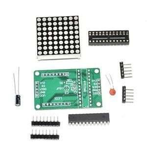
This chip is often used to drive 7-segment display having up to 8 digits or up to 64 individual LEDs. It is not unusual find this chip in DIY kits to be mounted on a small PCBs like that used in this article (See Fig. 1).
This chip could be found in different packages and uses a non-standard SPI (Data is clocked even if CS remains high but is needed a low to high transition to complete communication.If you are not familiar with SPI communication read Meeting SPI). MAX7221 is similar to MAX7219 except for two parameters:
- MAX7221 segment drivers are slew-rate limited to reduce electromagnetic interference;
- its serial interface is fully SPI compatible.
In theory our example could work with MAX7221 as well but it has been tested with MAX7219 only.
Documentation
The next document is the datasheet for both MAX7219 and MAX7221.
Features
Design and DIY kit connections
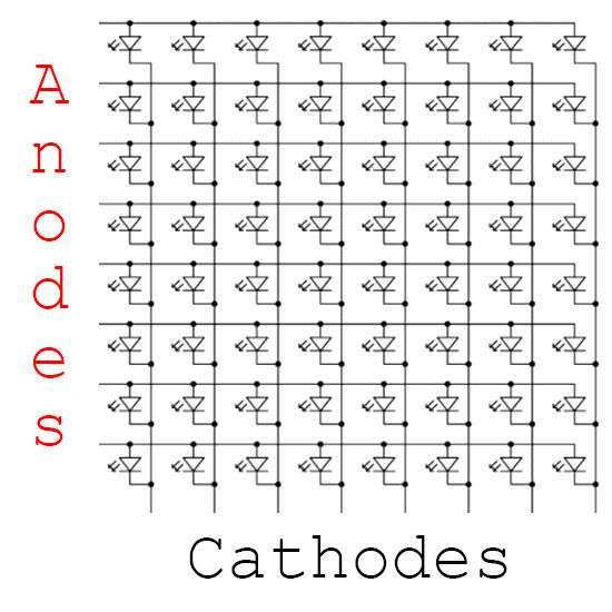
The MAX7219 can work with a voltage between 4.0~5.5V, and could be configured writing in some registers using a SPI. DIY kit we are using in this example is almost standard. the 8×8 LED Matrix provides 8 common cathodes and 8 common anodes identifying rows and columns of our matrix (See Fig. 2). Anodes are connected to segment outputs and cathodes to digits outputs. In MAX7219, when a segment driver is turned on it is pulled to V+ and when a digit driver is turned on it is pulled to GND.
If we consider the matrix orientation as that from Fig.1, segments (i.e. anodes) are representative of row indexes and digits (i.e. cathodes) are representative of column indexes. So if segment C and digit 0 are turned on the first LED on the third row is on. Combining the possible values for digits and segments MAX7219 can address each LED individually. Note that we have not to perform some kind of multiplexing or scan as it is already performed internally by MAX7219.
On the PCB we should find some capacitors to minimize power-supply ripple and a resistor to setup output current. In our case we have a 10μF electrolytic and a 0.1μF ceramic capacitor (between V+ and GND pins from MAX7219) and a 10kΩ resistor (between V+ and ISET pins from MAX7219). Current for a segment driver (i.e. current for an entire row) is typically 100 times the RSET current (that could be computed as V+/RSET = 5V / 10kΩ = 0.5mA).
Pin description
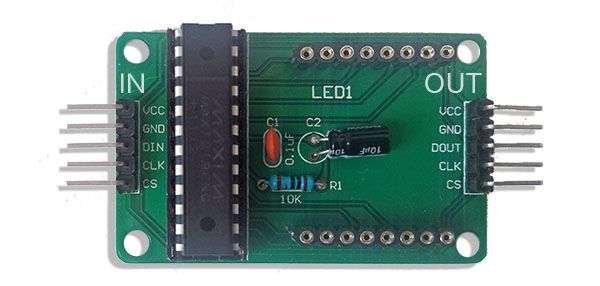
Not every pin from MAX7219 is connected to the external connector. These devices could be connected in chain so we have two connectors. For the input one we have starting from top:
- VCC, power supply 4.0~5.5V DC
- GND, connection to ground
- DIN, SPI master output slave input
- SCL, SPI serial clock
- CS, SPI chip select
For the output one we have starting from top:
- VCC, power supply 4.0~5.5V DC
- GND, connection to ground
- DOUT, SPI master input slave output
- SCL, SPI serial clock
- CS, SPI chip select
Note that DOUT could be connected to SPI MISO closing daisy chain or to DIN of another MAX7219.
Operation mode
Communication scheme and timing
Communication occurs through SPI bus. Summarizing most important info about communication are:
- CPOL is low;
- CPHA is low;
- Clock maximum rate is 10MHz;
- Data size is 16 bit;
Registers
The MAX7219 has several 8-bit register in which we can write using a word like that shown in Fig.4. As example writing this:
uint16_t txbuf = {a << 8 | b};
spiSelect(spip);
spiSend(spip, 1, &txbuf);
spiUnselect(spip);
we are writing b in the register pointed by a. We have a register for each digit and 6 control registers.
Digit 0~7
These are data register for the 8 digit which MAX7219 is managing. Meaning of this registers depends on DECODE MODE.
Decode mode
This register sets BCD code B or no-decode operation for each digit. Code B is a decode option that allow to easily draw certain symbols on a 7-segment display. So, if this option is enabled, writing 0x02 in Digit 0 register certain segments will be turned on drawing a number “2” on the first digit of our display. In Code B mode the allowed symbols are digits from “0” to “9”, “E”, “H”, “L”, “P” and “-” (See Table 5 on datasheet for more informations).Note that as we are driving a LED matrix decode option does not have any sense. In no-decode mode every bit represents a segment (as shown in Table 6 on datasheet).
Intensity
We already said that MAX7219 allows display brightness to be controlled through RSET. Display brightness can also be controlled digitally using intensity register. Digital control of display brightness is provided by an internal pulse-width modulator. The modulator scales the average segment current in 16 steps from a maximum of 31/32 down to 1/32 of the peak current set by RSET (For more info see table 7 on datasheet).
Scan Limit
We already said the MAX7219 performs multiplexing. Thus register sets the number of digits scanned during this operation. Multiplexing is done with a typical scan rate of 800Hz when all digits are scanned. The less digits are scanned the more frequency and display brightness increases: for that reason scan-limit register should not be used to blank portions of the display.
Shut Down
The Shut Down register operates in two modes: normal mode and shut down mode. In shut down mode, the scan oscillator is halted, all segment current sources are pulled to ground, and all digit drivers are pulled to V+, thereby blanking the display. Data in the digit and control registers remains unaltered so we can write operate on register even if MAX7219 is in shut down mode. This mode can be used to save power or to flash the display by successively entering and leaving normal mode.
Display test
The display-test register operates in two modes: normal and display test. Display-test mode turns all LEDs on by overriding, but not altering, all controls and digit registers
(including the shut-down register). In display-test mode, 8 digits are scanned and the duty cycle is 31/32 (See Table 10 on datasheet for more information).
No Operation
This register is used when more devices are connected in daisy chain. Imagine we have 3 devices connected and we want to edit a digit on the last device. We have to send anyway three words. To avoid unwanted changes to the first and the second device we can use their No Operation register writing in it. As example let’s consider next codebox:
uint16_t txbuf[3] = {0xC0, 0x00, 0x00};
spiSelect(spip);
spiSend(spip, 3, txbuf); /* Most Significant Word First */
spiUnselect(spip);
Proposed demo
This demo is a simple accomplishment of what we said above.
Demo explained
In the demo shown in the video above we set up MAX7219 as normal operation, no-decode mode, scanning each digit with the maximum display intensity. After that we just copy some pre-sets in the Digit registers.
To do this we just need to start SPI with proper configuration to write in registers. This operation is performed through an spiSend(). Some times ago we wrote bit masks and a write register function for MAX7219. We put this code in the community repository so you can find it under C:\ChibiStudio\chibios3\community\os\various\devices_lib\others. Just note, we fixed some bugs in MAX7219_DM_t enumeration and they will be updated from version 3.0.1 of ChibiOS. Anyway this bug doesn’t impact this demo.
/*
    PLAY Embedded demos - Copyright (C) 2014-2016 Rocco Marco Guglielmi

    This file is part of PLAY Embedded demos.

    Licensed under the Apache License, Version 2.0 (the "License");
    you may not use this file except in compliance with the License.
    You may obtain a copy of the License at

        http://www.apache.org/licenses/LICENSE-2.0

    Unless required by applicable law or agreed to in writing, software
    distributed under the License is distributed on an "AS IS" BASIS,
    WITHOUT WARRANTIES OR CONDITIONS OF ANY KIND, either express or implied.
    See the License for the specific language governing permissions and
    limitations under the License.
*/

/*
    Tested under ChibiOS/RT 3.0.1, Project version 1.0
 */
#include "ch.h"
#include "hal.h"
#include "max7219.h"

/*===========================================================================*/
/* LED Matrix related code.                                                  */
/*===========================================================================*/

#define MAX_PRESET_NUMB                         17
#define MAX_DIGITS                              8

static uint8_t presets[MAX_PRESET_NUMB][MAX_DIGITS] = {
   {0x18, 0x18, 0x18, 0x99, 0xDB, 0x7E, 0x3C, 0x18}, /**< Arrow dx.         */
   {0x18, 0x3C, 0x7E, 0xDB, 0x99, 0x18, 0x18, 0x18}, /**< Arrow sx.         */
   {0x00, 0x20, 0x44, 0x40, 0x40, 0x44, 0x20, 0x00}, /**< Happy face.       */
   {0x00, 0x20, 0x14, 0x10, 0x10, 0x14, 0x20, 0x00}, /**< Sad face.         */
   {0x00, 0x00, 0x00, 0xDF, 0xDF, 0x00, 0x00, 0x00}, /**< Exclamation point.*/
   {0x24, 0x66, 0xE7, 0xE7, 0xE7, 0xE7, 0x66, 0x24}, /**< Negate.           */
   {0x00, 0x84, 0x86, 0xFF, 0xFF, 0x80, 0x80, 0x00}, /**< 1.                */
   {0x00, 0x86, 0xC7, 0xE1, 0xB1, 0x9F, 0x8E, 0x00}, /**< 2.                */
   {0x00, 0x00, 0x42, 0xC3, 0xDB, 0xFF, 0x66, 0x00}, /**< 3.                */
   {0x00, 0x3F, 0x3F, 0x20, 0x20, 0xF8, 0xF8, 0x00}, /**< 4.                */
   {0x00, 0xDF, 0xDB, 0xDB, 0xDB, 0xFB, 0x71, 0x00}, /**< 5.                */
   {0x00, 0x7E, 0xFF, 0x89, 0x89, 0x89, 0x70, 0x00}, /**< 6.                */
   {0x00, 0x03, 0x03, 0xE3, 0xFB, 0x1F, 0x07, 0x00}, /**< 7.                */
   {0x00, 0x76, 0xFF, 0x99, 0x99, 0xFF, 0x76, 0x00}, /**< 8.                */
   {0x00, 0x8E, 0x91, 0x91, 0x91, 0xFF, 0x7E, 0x00}, /**< 9.                */
   {0x00, 0x7E, 0xFF, 0x81, 0x81, 0xFF, 0x7E, 0x00}, /**< 0.                */
   {0x00, 0x06, 0x76, 0x30, 0x30, 0x76, 0x06, 0x00}  /**< Creeper face.     */
};

/*===========================================================================*/
/* SPI related code.                                                         */
/*===========================================================================*/

#define  GPIOB_SPID1_CS                 6
#define  GPIOA_SPID1_SCK                5
#define  GPIOA_SPID1_MISO               6
#define  GPIOA_SPID1_MOSI               7

static const SPIConfig spicfg = {
  NULL,
  GPIOB,                                          /*   port of CS  */
  GPIOB_SPID1_CS,                                 /*   pin of CS   */
  SPI_CR1_BR | SPI_CR1_DFF                        /*   CR1 register */
};

/*===========================================================================*/
/* Generic code.                                                             */
/*===========================================================================*/
 static unsigned ii, jj;

/*
 * Application entry point.
 */
int main(void) {


  /*
   * System initializations.
   * - HAL initialization, this also initializes the configured device drivers
   *   and performs the board-specific initializations.
   * - Kernel initialization, the main() function becomes a thread and the
   *   RTOS is active.
   */
  halInit();
  chSysInit();

  /*
   * SPID1 I/O pins setup.(It bypasses board.h configurations)
   */
  palSetPadMode(GPIOA, GPIOA_SPID1_SCK,
                PAL_MODE_ALTERNATE(5) | PAL_STM32_OSPEED_HIGHEST);   /* New SCK */
  palSetPadMode(GPIOA, GPIOA_SPID1_MISO,
                PAL_MODE_ALTERNATE(5) | PAL_STM32_OSPEED_HIGHEST);   /* New MISO*/
  palSetPadMode(GPIOA, GPIOA_SPID1_MOSI,
                PAL_MODE_ALTERNATE(5) | PAL_STM32_OSPEED_HIGHEST);   /* New MOSI*/
  palSetPadMode(GPIOB, GPIOB_SPID1_CS,
                PAL_MODE_OUTPUT_PUSHPULL | PAL_STM32_OSPEED_HIGHEST);/* New CS  */

  spiStart(&SPID1, &spicfg);
  max7219WriteRegister(&SPID1, MAX7219_AD_DISPLAY_TEST, FALSE);
  max7219WriteRegister(&SPID1, MAX7219_AD_SHUTDOWN, MAX7219_OM_Normal);
  max7219WriteRegister(&SPID1, MAX7219_AD_SCAN_LIMIT, MAX7219_SL_7);
  max7219WriteRegister(&SPID1, MAX7219_AD_DECODE_MODE,
                       MAX7219_DM_No_decode);
  max7219WriteRegister(&SPID1, MAX7219_AD_INTENSITY,
                       MAX7219_IM_31_32);
  while (TRUE) {

    for(ii = 0; ii < MAX_DIGITS; ii++) {

      max7219WriteRegister(&SPID1, MAX7219_AD_DIGIT_0 + (ii << 8),
                           presets[jj][ii]);
    }
    jj = (jj + 1) % MAX_PRESET_NUMB;
    chThdSleepMilliseconds(500);
  }
  spiStop(&SPID1);
}
Project download
The attached demo has been tested under ChibiOS 20.3.x.
Be the first to reply at STM32, ChibiOS and a 8×8 LED Matrix